Dual carrier for joining IC die or wafers to TSV wafers

a dual carrier and ic die technology, applied in the direction of adhesives, electrical devices, semiconductor devices, etc., can solve the problems of reducing the resistance of the joints, and complicating the jointing/bonding with the ic die. , to achieve the effect of improving the circuit performance and reliability of singulated stacked ic dies, reducing the contact resistance of the joints, and reducing the warpage/bow significantly

Active Publication Date: 2011-07-28
TEXAS INSTR INC
View PDF6 Cites 41 Cited by
  • Summary
  • Abstract
  • Description
  • Claims
  • Application Information

AI Technical Summary

Benefits of technology

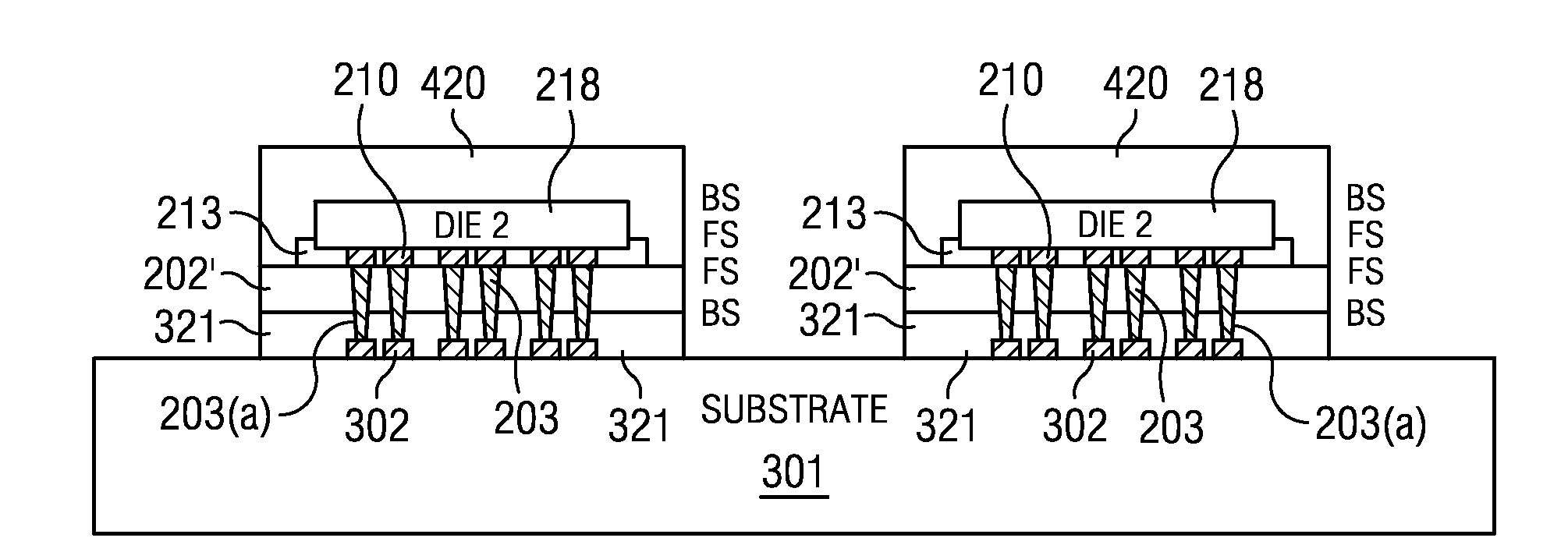
[0009]At least one second IC die which can comprise singulated IC die or a wafer is then bonded to the plurality TSV die on the top side of the thinned TSV wafer to form a stacked TSV wafer comprising electronic article. Since the TSV wafer is supported by the second carrier wafer during bonding of the singulated IC die or wafer, warpage / bow is significantly reduced which reduces the contact resistance of the joints, and as a result improves circuit performance and reliability of singulated stacked IC die generated by singulation (e.g. sawing) of the stacked TSV wafer comprising electronic article.

Problems solved by technology

Problems with this conventional sequential stacked die assembly technique include difficulties with die-to die jointing via bumps because the first IC die mounted on the package substrate may have significant warpage / bow.
In addition, since both IC die are thinned and the top sides are exposed during assembly, IC die handling is generally difficult and can result in yield loss due to cracked IC die or scratching of the IC die.
However, warpage of the thinned TSV wafer can complicate jointing / bonding with the IC die.
For example, as known in the art, warpage results in misaligned joints which reduces contact area which increases contact resistance of the joint, particularly for fine pitched pads, and can even cause open circuited contacts.
Moreover, conventional thin die-wafer stacks are difficult to handle which can result in scratching and a tendency to crack.
Due to warpage / bending of the TSV wafer during TSV tip exposure which increases as the wafer thinning precedes, this second known D2W method can result in significant TSV tip height variation including significant height variation across individual IC die which can cause bonding problems during subsequent bonding of the TSV tips of the die stack to a package substrate.

Method used


Image

  • Dual carrier for joining IC die or wafers to TSV wafers
  • Dual carrier for joining IC die or wafers to TSV wafers
  • Dual carrier for joining IC die or wafers to TSV wafers

Examples


examples

[0039]Embodiments of the invention are further illustrated by the following specific Examples, which should not be construed as limiting the scope or content of embodiments of the invention in any way.

[0040]FIG. 5 is a graph of viscosity vs. temperature (° C.) for three different exemplary adhesive materials that can generally be used as the bonding adhesives described herein. Adhesive A can be used for the lower debonding temperature adhesive, and adhesives B or C for the higher debonding temperature adhesive. Softening temperature as used herein refers to the temperature at which the viscosity is the minimum viscosity required to stand against debonding, such at least 200 Pa·S. Curve A is the viscosity curve for the Brewer Science WaferBOND™ HT-10.10 coating manufactured by Brewer Science, Inc., Springfield, Mo. Curves B and C provide other viscosity curves for other materials that provide a higher debonding temp as compared to that shown in Curve A.

[0041]One exemplary higher debo...


PUM


Abstract

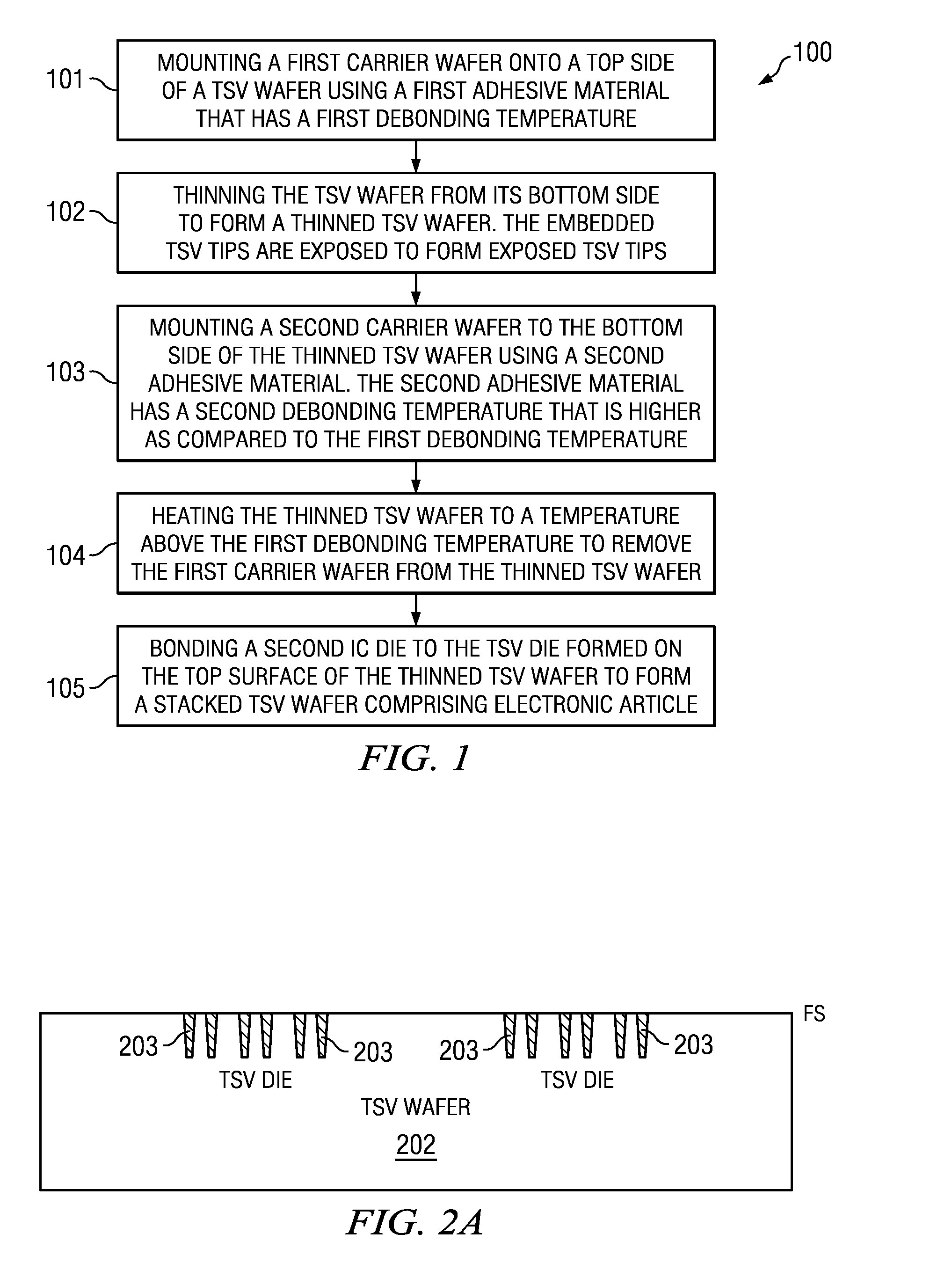
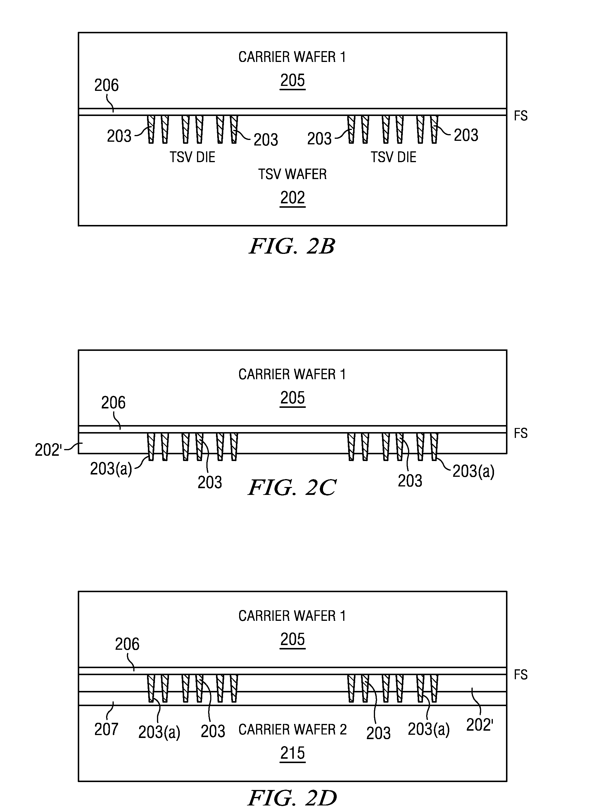
A method of forming stacked electronic articles using a through substrate via (TSV) wafer includes mounting a first carrier wafer to a top side of the TSV wafer using a first adhesive material that has a first debonding temperature. The TSV wafer is thinned from a bottom side of the TSV wafer to form a thinned TSV wafer. A second carrier wafer is mounted to the bottom side of the TSV wafer using a second adhesive material that has a second debonding temperature that is higher as compared to the first debonding temperature. The thinned TSV wafer is heated to a temperature above the first debonding temperature to remove the first carrier wafer from the thinned TSV wafer. At least one singulated IC die is bonded to TSV die formed on the top surface of the thinned TSV wafer to form the stacked electronic article.

Description

FIELD[0001]Disclosed embodiments relate to integrated circuit (IC) assembly processing, and more particularly to bonding die or wafers to TSV comprising wafers.BACKGROUND[0002]In order to stack IC die in a face-to-face manner using standard flip-chip assembly techniques, the assembly is conventionally performed in a sequential manner by bonding a first thinned IC die then a second thinned IC die (e.g., a thinned die 25 to 150 μm thick) onto a package substrate (e.g., PCB). In a typical arrangement, the first IC die can be a TSV comprising die that is mounted face (i.e. active circuit / top side) up on the surface of a package substrate where the TSVs form joints with pads on the package substrate surface. Capillary underfill is then generally performed. The second IC die is then generally flip-chip (FC) mounted to the top side of the first IC die.[0003]Problems with this conventional sequential stacked die assembly technique include difficulties with die-to die jointing via bumps beca...

Claims


Application Information

Patent Timeline
Patent Type & Authority Applications(United States)
IPC IPC(8): H01L21/60
CPCC09J5/06C09J2203/326H01L2924/0002H01L2924/00014H01L2924/1461H01L2224/0401H01L2224/81191H01L2924/014H01L2924/01043C09J2205/302H01L21/561H01L21/565H01L21/6836H01L21/76898H01L24/11H01L24/13H01L24/16H01L24/81H01L24/94H01L24/97H01L25/0657H01L25/50H01L2221/6834H01L2221/68381H01L2224/0557H01L2224/13009H01L2224/81001H01L2224/81203H01L2224/81801H01L2224/83191H01L2224/83192H01L2224/97H01L2225/06513H01L2225/06517H01L2225/06541H01L2924/01029H01L2924/01079H01L2924/19041H01L2924/20105H01L2924/01005H01L2924/01006H01L2924/01033H01L2924/01042H01L2224/81H01L2924/00H01L2224/05552H01L2924/181H01L2924/14C09J2301/502
Inventor TAKAHASHI, YOSHIMIMURTUZA, MASOODDUNNE, RAJIVCHAUHAN, SATYENDRA SINGH
Owner TEXAS INSTR INC
Why Eureka
Try Eureka