Defect estimation device and method and inspection system and method

a technology of defect estimation and inspection system, applied in the direction of instruments, photomechanical equipment, image enhancement, etc., can solve the problems of difficult to distinguish a difference between a shape defect of a pattern and a potentially existing shape error of a pattern, and the position error of an extremely small pattern is required to be inspected

Active Publication Date: 2011-08-04
NUFLARE TECH INC
View PDF7 Cites 47 Cited by
  • Summary
  • Abstract
  • Description
  • Claims
  • Application Information

AI Technical Summary

Benefits of technology

[0034]In another aspect of this invention, an inspection device, which irradiates light to a mask formed with a pattern, forming an image of the mask on an image sensor through an optical system, and determines the presence of a defect, comprising: an optical image acquisition part which obtains an optical image of the mask from the image sensor; a first estimation part which estimates, from a reference image as a reference of the determination and the optical image, each first pattern image of the patterns transferred to a substrate by a lithography process; a first comparison part which compares the first pattern images with each other and, when a difference exceeds at least one of the threshold values, determines that there is a defect; a simulated repair part which simulates a repair to the optical image at a portion determined as defective by the comparison; and a second estimation part which estimates each second pattern image of the patterns, transferred onto the substrate, from the reference image and the simulated optical image, wherein in the second pattern image, the lithography process is more advanced than that in the first pattern image.

Problems solved by technology

Therefore, in the mask inspection, the dimension of the pattern defect is miniaturized, and a positional error of an extremely small pattern is required to be inspected.
However, this method cannot detect a defect common to both compared patterns.
However, with the recent miniaturization of a device pattern on a mask, it is difficult to distinguish a difference between a shape defect of a pattern and a potentially existing shape error of a pattern.
Incidentally, defects associated with micropatterns include not only shape defects typified by pattern edge roughness, but also pattern linewidth errors and pattern displacement errors, which are becoming more and more significant due to the miniaturization of device patterns.
Therefore, there has been a strong need to accurately control the dimensions of patterns, thus increasing the difficulty of manufacturing masks.
As a result, there has been a loss in the yield of masks that meet the required specifications, thereby raising mask manufacturing cost.
Further, the required accuracy of a linewidth or pattern of a mask increases, whereby determination as to whether or not there is a defect is difficult if the only comparison is between generated reference data based on design pattern data and a pattern image taken by an inspection device.
That is to say, according to a determination method based on a transfer image, it can be predicted that the shape defect of a mask makes the transfer image incorrect.
However, in this case, there is a problem that it cannot be indicated which of the defect portions in the assist pattern, that is, which of a plurality of fracture portions causes the constriction of the line width in the main pattern, or which combination of the plurality of fracture portions causes the constriction of the line width in the main pattern.
However, in the prior art there is no inspection device which can indicate the level of influence that a defect will have on the wafer.
Furthermore, there is no inspection device that can determine whether the repair of a specific pattern error or repair of a combination of pattern errors in the wafer transfer image will result in an acceptable transfer image to the wafer.

Method used


Image

  • Defect estimation device and method and inspection system and method
  • Defect estimation device and method and inspection system and method
  • Defect estimation device and method and inspection system and method

Examples


embodiment 1

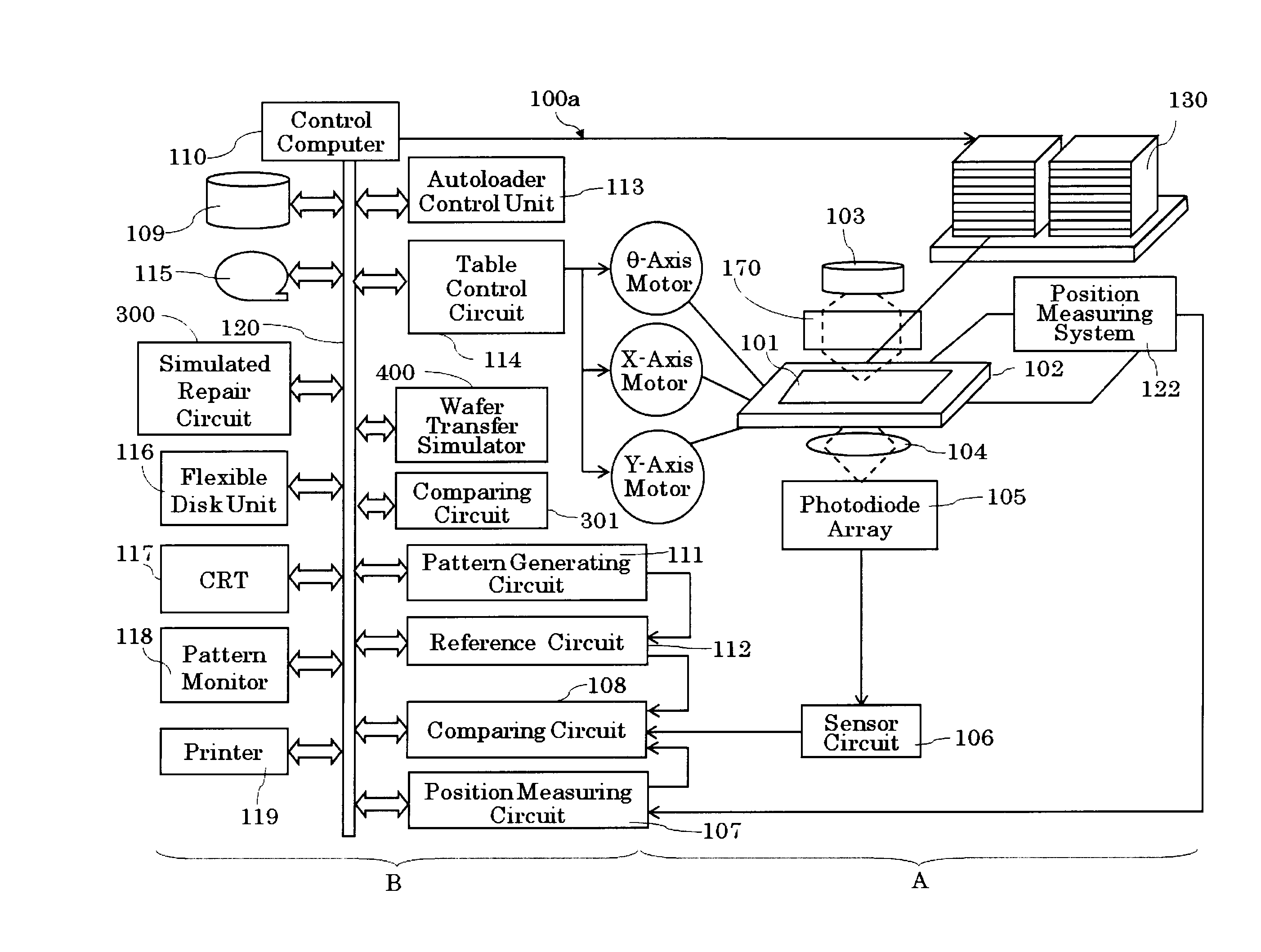
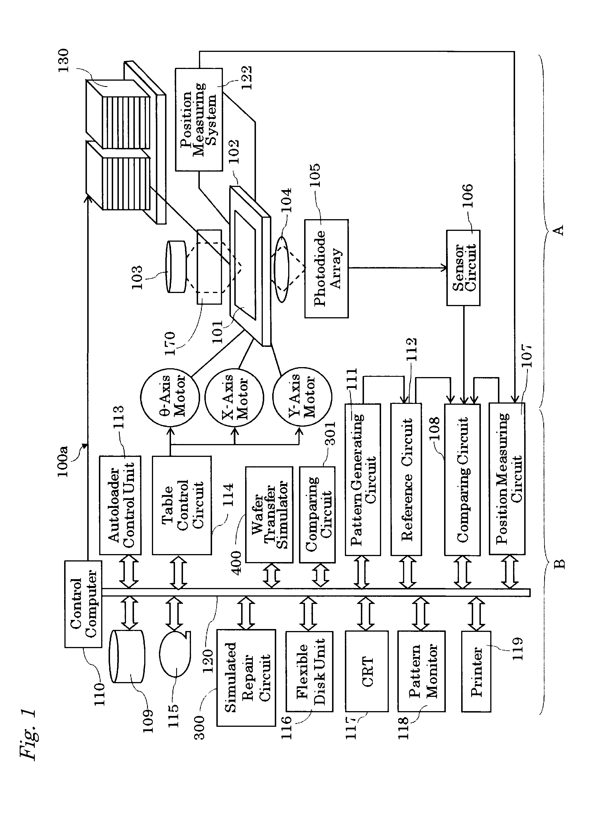
[0071]FIG. 1 is a diagram showing the configuration of an inspection system according to an Embodiment of the present invention. The inspection system of the present Embodiment will be described in connection with the inspection of masks used in photolithography.

[0072]As shown in FIG. 1, the inspection system 100a includes an optical image capture unit A and a control unit B.

[0073]The optical image capture unit A includes an irradiating laser beam light source 103, an XYθ table 102 movable in the horizontal X and Y directions and rotatable in a horizontal plane (or in a θ direction), an optical illumination system 170 serving as a transmission illumination system, an enlarging optical system 104, a photodiode array 105, a sensor circuit 106, a position measuring system 122, and an autoloader 130.

[0074]In the control unit B, a control computer 110 which controls the entire inspection system 100a is connected through a bus 120 (serving as a data transmission path) to a position measur...

embodiment 2

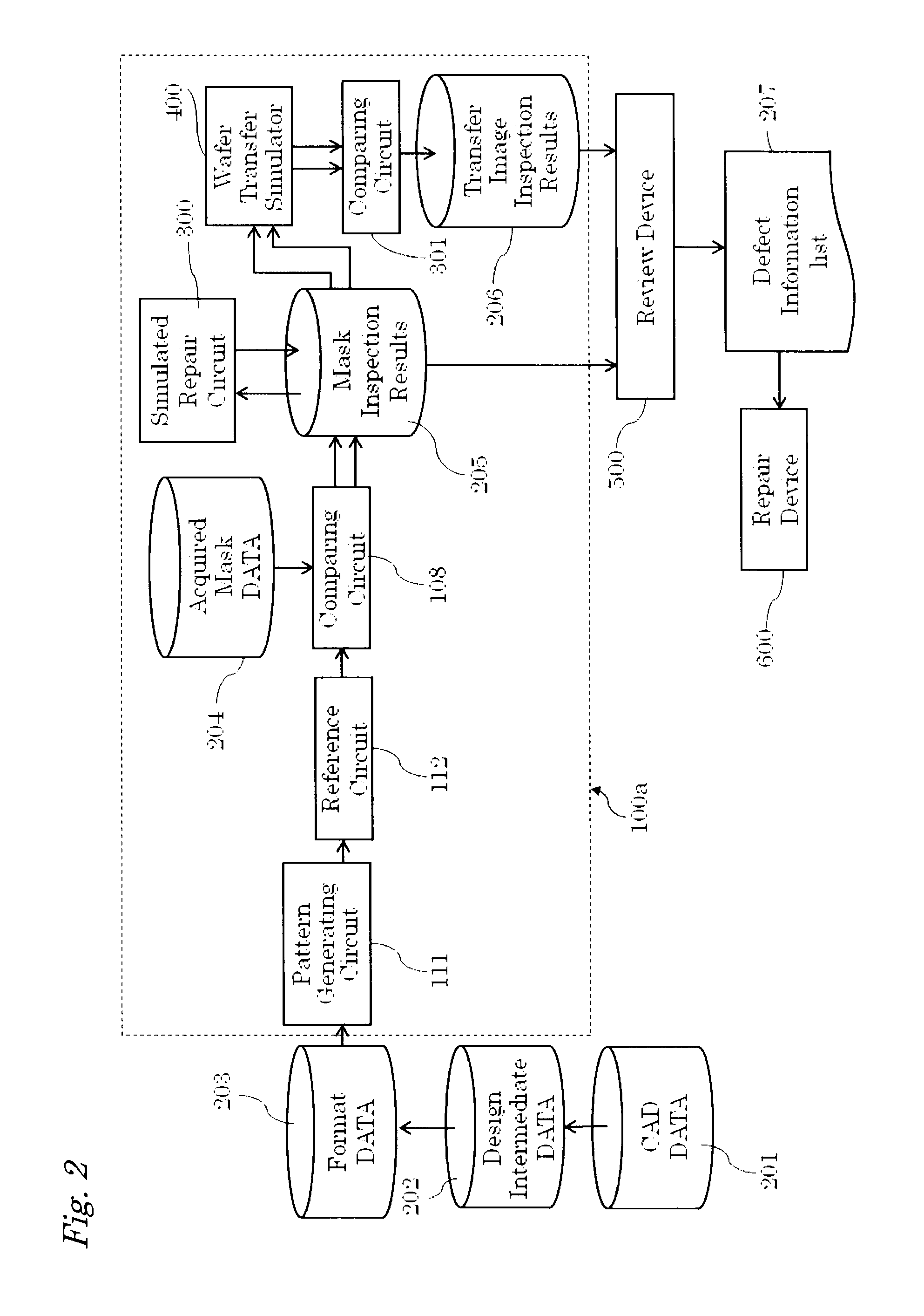
[0140]FIG. 5a is an example of the mask shape defect. In this example, there is a fracture of an assist pattern 1002 in a region 1003. The assist pattern 1002 is a pattern, which is auxiliary provided in a mask for the purpose of improving the patterning characteristics of a main pattern 1001. The assist pattern 1002 itself is not transferred onto a wafer. When a wafer transfer image on the mask of FIG. 5a is estimated by simulation, the wafer transfer image shown in FIG. 5b is obtained. That is to say, in the wafer transfer image, the line width at the defect portion is smaller than the line width of a pattern at a normal portion. When the degree of reduction in the line width is more than a specified value, a region 1004 is determined as the defect portion to be repaired. The degree of reduction in the line width may be specified by a difference of an estimated line width between the normal portion and the defect portion or may be specified by the ratio of the estimated line width...


PUM

PropertyMeasurementUnit
lengthaaaaaaaaaa
defectaaaaaaaaaa
optical imageaaaaaaaaaa

Abstract

Acquired mask data of a defect portion is sent to a simulated repair circuit 300 to be simulated. The simulation of the acquired mask data 204 is returned to the mask inspection results 205 and thereafter sent to a wafer transfer simulator 400 along with a reference image at the corresponding portion. A wafer transfer image estimated by the wafer transfer simulator 400 is sent to a comparing circuit 301. When it is determined that there is a defect in the comparing circuit 301, the coordinates and the wafer transfer image which is a basis for the defect determination are stored as transfer image inspection results 206. The mask inspection results 205 and the transfer image inspection result 206 are then sent to the review device 500.

Description

BACKGROUND OF THE INVENTION[0001]1. Field of the Invention[0002]The present invention relates to a defect estimation device and method used to estimate defects of a pattern formed on an object to be inspected such as a mask, and an inspection system and inspection method used to detect defects of a pattern formed on an object to be inspected.[0003]2. Background Art[0004]In recent years, as the levels of integration and capacity of large scale integrated circuits (LSIs) have increased, there has been a need to continue to reduce the width of the circuit patterns of semiconductor devices. Semiconductor devices are manufactured by a reduced projection exposure apparatus called a “stepper” using original artwork patterns with a circuit pattern formed thereon, these are called masks or reticles (hereinafter referred to collectively as masks). Specifically, a pattern on a mask is transferred to the wafer by exposure to light, thereby forming circuits on to a wafer. Masks used to transfer ...

Claims


Application Information

Patent Timeline
Patent Type & Authority Applications(United States)
IPC IPC(8): G06K9/00G01N21/956G01N23/225G03F1/84
CPCG06T7/001G06T7/0002G06T2207/30148G06V10/42G03F1/84G01N21/95607G03F7/7065
Inventor TSUCHIYA, HIDEOABE, TAKAYUKI
Owner NUFLARE TECH INC
Why Eureka
Try Eureka