Method for manufacturing an electronic device

Active Publication Date: 2011-08-04
NXP BV
View PDF17 Cites 2 Cited by
  • Summary
  • Abstract
  • Description
  • Claims
  • Application Information

AI Technical Summary

Benefits of technology

[0013]The method according to the present invention allows for a process of manufacturing an electronic device and in particular smart cards for RFID applications, in which the application of mechanical stress on the chip during the step of connecting the conductive structure to the contacting surface of the integrated circuit is minimized. Connecting is performed via the hole in the at least one substrate layer, which is formed in the substrate layer prior to the connecting step so that the connecting step itself is not affected by any material displacement and any mechanical stress related thereto.
[0014]Since the chip is not compressed while contacting it with the antenna, the risk of formation of cracks is minimized. Since the chip is not exposed to mechanical stress, it can be designed thinner than those known from the state of the art and essential and, as the case may be, delicate structures of the chip can also be arranged in the region of the contacting surfaces. This allows for a smaller overall design of the chip.
[0015]Forming the conductive structure, e.g. the antenna structure, on a surface of a substrate layer and connecting it to the chip in a single process step provides a highly effective and economic process.
[0016]According to a particularly preferred embodiment of the inventive method, said step of forming a conductive structure on a surface of said at least one substrate layer and of connecting said conductive structure to said contacting surface comprises printing said structure with a conductive ink and during said printing filling said hole with ink thereby connecting the conductive structure with the connecting surface. Such a process is particularly easy to perform with known devices already used for printing antenna structures on substrate layers. The conductive ink, when applied in the region of the hole formed above the contact surface, naturally flows into the hole, thereby establishing contact with the contacting surface. In this way, said steps of forming a conductive structure and of connecting said conductive structure with the connecting surfaces of the integrated circuit can easily be performed in a single process step.
[0018]In this connection, in a particularly advantageous embodiment of the present invention, said step of connecting said conductive structure to said contacting surface comprises applying a conductive paste or a conductive adhesive into the hole, whereby a particularly simple mode of establishing contact between the conductive antenna structure and the contacting surface of the chip is achieved while at the same time safe and durable contacting can be safeguarded.
[0021]According to a preferred embodiment of the present invention said step of forming a hole is performed before the step of arranging said integrated circuit between the two layers of said substrate. In this way, handling is facilitated and the risk of negatively affecting the integrated circuit during the application of laser radiation is minimized.

Problems solved by technology

In such a process, the step of providing the antenna structure on a surface of the substrate layer and the step of contacting the antenna structure with the chip are separate, thereby giving rise to procedural inconvenience.
Structures using direct chip attach reveal the disadvantage that the IC is more or less unprotected during the lamination process, which limits the IC thickness to around 100 μm in order to give reasonable die strength values.

Method used


Image

  • Method for manufacturing an electronic device
  • Method for manufacturing an electronic device

Examples


Embodiment Construction

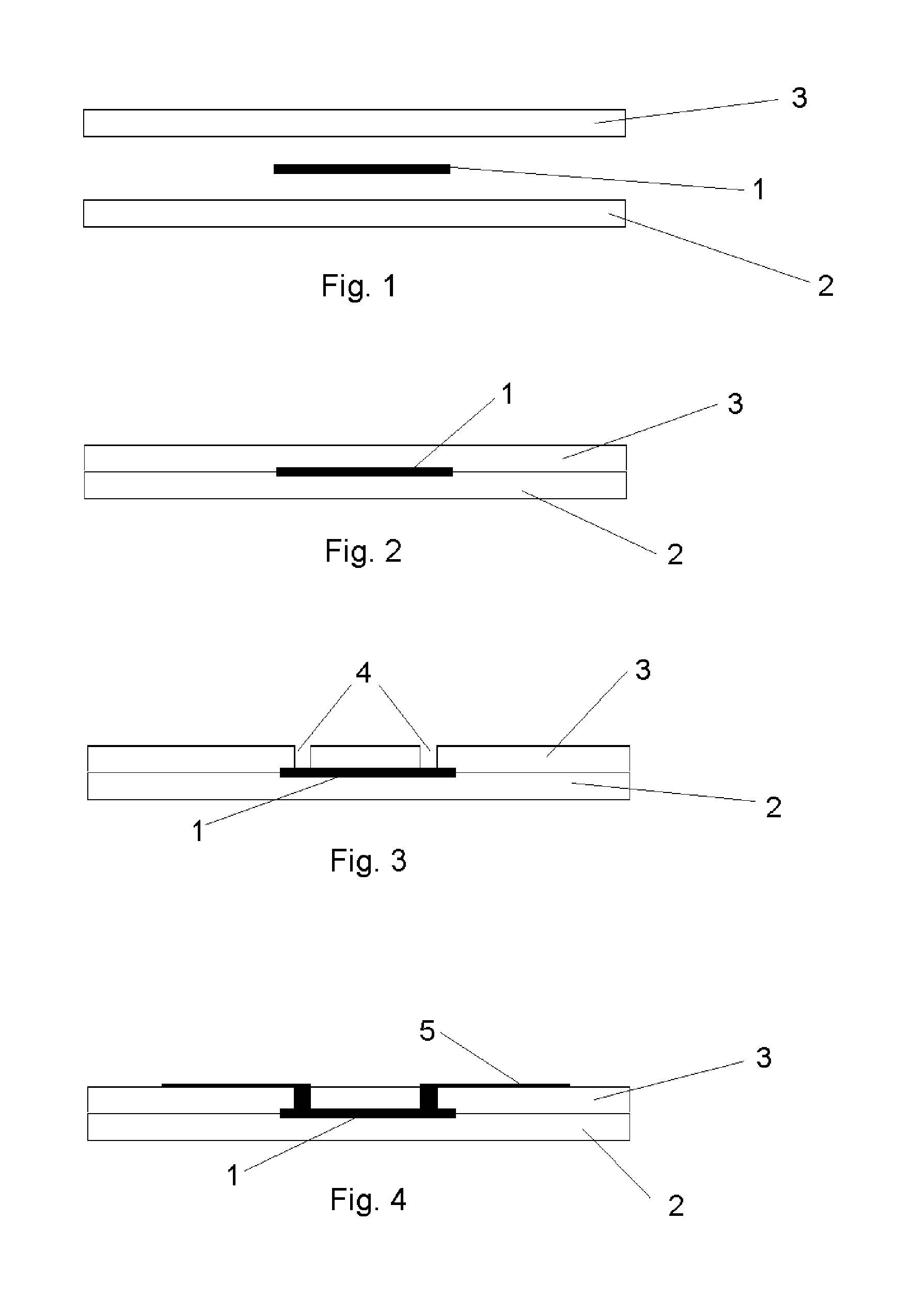
[0030]In FIG. 1 an integrated circuit (IC) 1 is arranged between a first substrate layer 2 and a second substrate layer 3. The IC 1 can be attached either by using glue or directly to the substrate material by using thermal or ultrasonic processes. This arrangement is then laminated to give the structure as shown in FIG. 2. Due to the low IC 1 thickness the substrate layers 2,3 are nearly parallel and the IC 1 is hermetically sealed and well protected by the substrate layers 2,3.

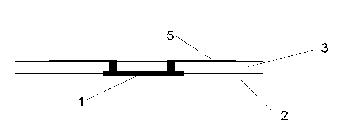
[0031]After this, holes 4 are made in the substrate layer 3 above the contacting surfaces of the IC 1 to give a structure as shown in FIG. 3. The contacting surfaces of the IC 1, such as, e.g., bond pads or bumps, are now in open connection to the ambience.

[0032]After this, the conductive structure 5 is printed on the surface of the second surface layer 3 with a conductive ink, so that the formation of the conductive structure, e.g. the antenna, and its coupling to the IC 1 via conductive material in the hol...


PUM

PropertyMeasurementUnit
Electrical conductoraaaaaaaaaa
Metallic bondaaaaaaaaaa
Thermoplasticityaaaaaaaaaa

Abstract

In a method for manufacturing an electronic device an integrated circuit (1) is arranged between two layers (2, 3) of a substrate, said integrated circuit (1) having at least one contacting surface, a hole (4) is formed in at least one substrate layer (3) above said at least one contacting surface, a conductive structure (5) is formed on a surface of said at least one substrate layer (3) facing away from the integrated circuit (1) and said conductive structure (5) is connected to said contacting surface by means of said hole (4).

Description

FIELD OF THE INVENTION[0001]The invention relates to a method for manufacturing an electronic device.BACKGROUND OF THE INVENTION[0002]Electronic devices within the scope of the present invention and in particular smartcards for RFID applications usually consist of an IC, packaged in a module, which is then connected with an antenna and subsequently integrated into a cardbody. For standard cards, normally the module is attached to a substrate foil, in which the insulated wire antenna is embedded and attached by a welding process to the module. This substrate foil then is called an inlay, which, in a separate step, is laminated into the final RFID card.[0003]An alternative way to produce an inlay uses a so-called direct chip attach process. In that case, the antenna consists of a structured layer of a conductive material, such as a thin metal foil, conductive ink, a galvanic plated layer etc., and the IC is connected directly to the antenna via, e.g., a flip chip process.[0004]For exa...

Claims


Application Information

Patent Timeline
IPC IPC(8): H01L21/60
CPCH01L2224/211H01L2224/20H01L2224/04105H01L23/5389G06K19/07749Y10T29/49016H01L2924/014H01L2924/01082H01L24/19H01L23/49822H01L2924/14H01L2924/01033
Inventor ZENZ, CHRISTIAN
Owner NXP BV
Why Eureka
Try Eureka