Semiconductor device and method of manufacturing the same

a technology of semiconductor devices and semiconductors, applied in semiconductor devices, semiconductor/solid-state device details, electrical apparatus, etc., can solve problems such as difficulty in sufficiently miniaturizing the size of cellular phones

Inactive Publication Date: 2011-08-11
RENESAS ELECTRONICS CORP
View PDF5 Cites 53 Cited by
  • Summary
  • Abstract
  • Description
  • Claims
  • Application Information

AI Technical Summary

Benefits of technology

[0011]A semiconductor device comprises: a semiconductor chip where semiconductor elements such as a MOSFET (Metal Oxide Semiconductor Field Effect Transistor) and a multilayered wiring are formed; and a package so formed as to cover the semiconductor chip. The package has functions such as (1) electrically coupling semiconductor elements formed in the semiconductor chip with an external circuit and (2) protecting the semiconductor chip from outside environments such as humidity and temperature, and preventing the semiconductor chip from being broken by vibration or shock and preventing its property from being deteriorated. The package also has functions of (3) enabling easy handling of the semiconductor chip and (4) dissipating heat during the operation of the semiconductor chip, and maximizing the performance of the semiconductor element.
[0013]Furthermore, in order to reduce the package size, some of the semiconductor chips are embedded inside the wiring board (Embedded Package). Thus, by embedding some of the semiconductor chips in the wiring board, the number of semiconductor chips to be mounted over the surface of the wiring board can be reduced. As a result, the package can be reduced in size.
[0016]An object of the present invention is to provide, in regard to a semiconductor device having a multilayered wiring board where a semiconductor chip is embedded, a technology which allows the multilayered wiring board to be made thinner.
[0023]In a semiconductor device having a multilayered wiring board where a semiconductor chip is embedded, the multilayered wiring board can be made thinner.

Problems solved by technology

When these semiconductor chips are packaged separately, it has become difficult to sufficiently miniaturize the size of the cellular phone.

Method used


Image

  • Semiconductor device and method of manufacturing the same
  • Semiconductor device and method of manufacturing the same
  • Semiconductor device and method of manufacturing the same

Examples


embodiment 1

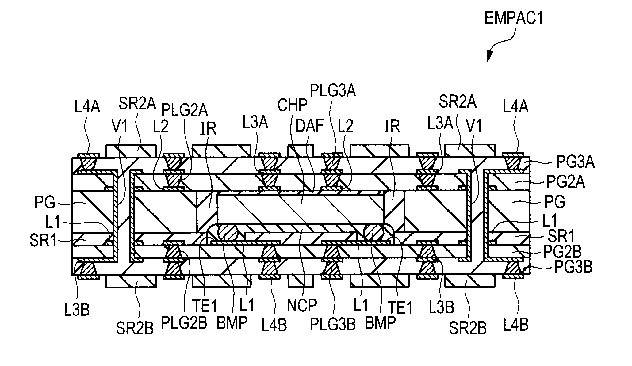
[0070]With reference to the drawings, a semiconductor device according to Embodiment 1 will be described. FIG. 1 is a cross-sectional view showing a configuration of a chip-embedded wiring board EMPAC1 according to Embodiment 1. In FIG. 1, with respect to the chip-embedded wiring board EMPAC1 according to Embodiment 1, a semiconductor chip CHP being a bear chip is embedded inside a multilayered wiring board in which a multilayered wiring is formed. To be specific, a wiring L1 is formed inside the multilayered wiring board, and a solder resist SR1 is formed so as to cover the wiring L1. Further, part of the wiring L1 is exposed from the solder resist SR1, and the exposed part of the wiring L1 serves as a terminal TE1.

[0071]The semiconductor chip CHP is mounted over the wiring L1 covered with the solder resist SR1. Semiconductor elements such as a MOSFET (Metal Oxide Semiconductor Field Effect Transistor) and the multilayered wiring are formed in the semiconductor chip CHP. The above ...

embodiment 2

[0092]In Embodiment 2, with reference to the drawings, an explanation will be given of a method for manufacturing the chip-embedded wiring board EMPAC1 described in Embodiment 1. In Embodiment 2, explanations will be given of the case where a gold bump electrode is used for the bump electrode to be formed over the semiconductor chip and the case where a solder bump electrode is used for the bump electrode to be formed over the semiconductor chip.

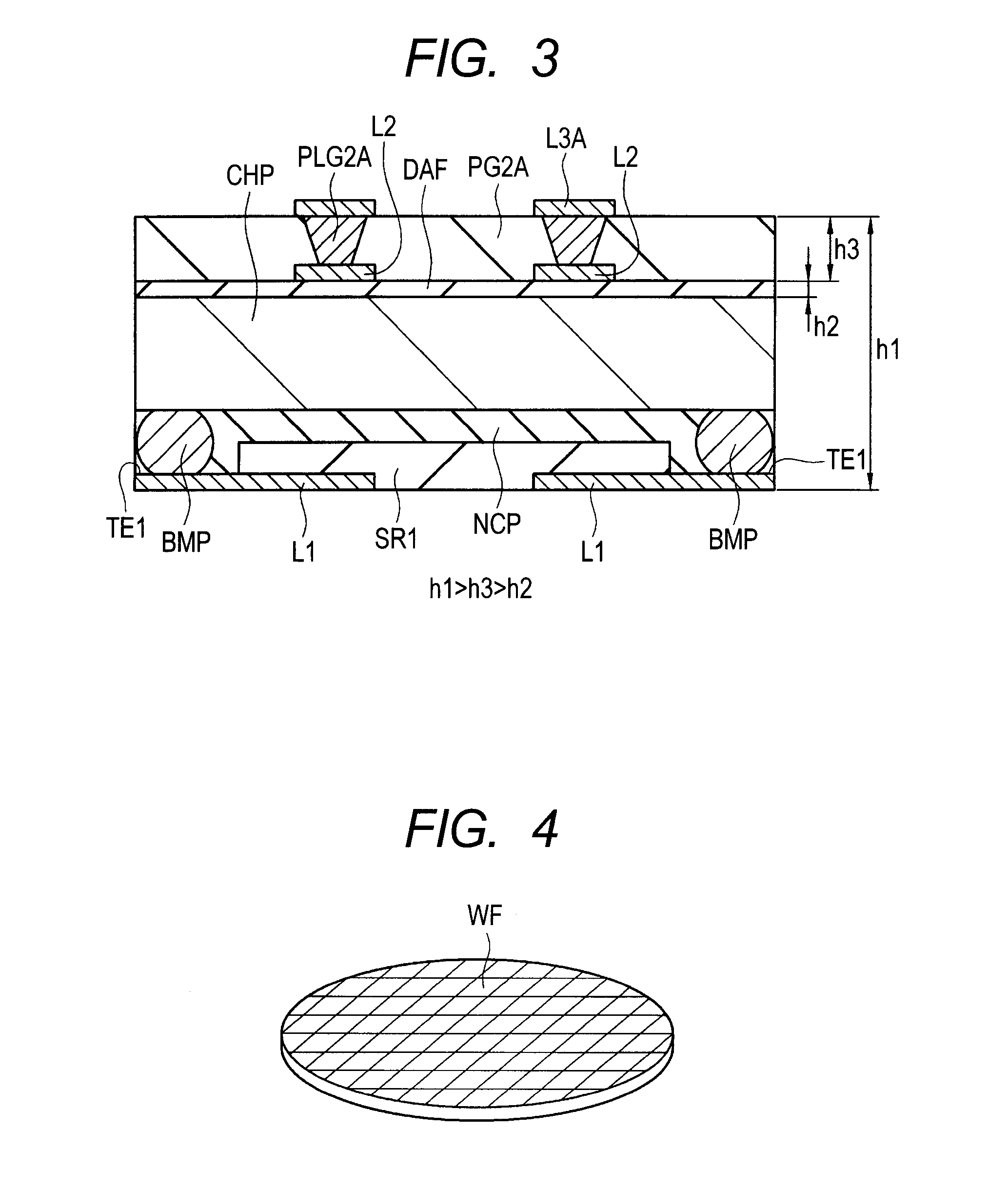
[0093]First, an explanation will be given of a method of forming the bump electrode over the semiconductor chip from the gold bump electrode. As shown in FIG. 4, a substantially disc-like semiconductor wafer WF is prepared. The semiconductor wafer WF is divided into a plurality of chip regions according to dicing lines formed in a scribe region. Over the main surface of the semiconductor wafer WF, for each partitioned chip region, there are formed semiconductor elements such as a MOSFET and multilayered wirings for coupling those semiconduct...

embodiment 3

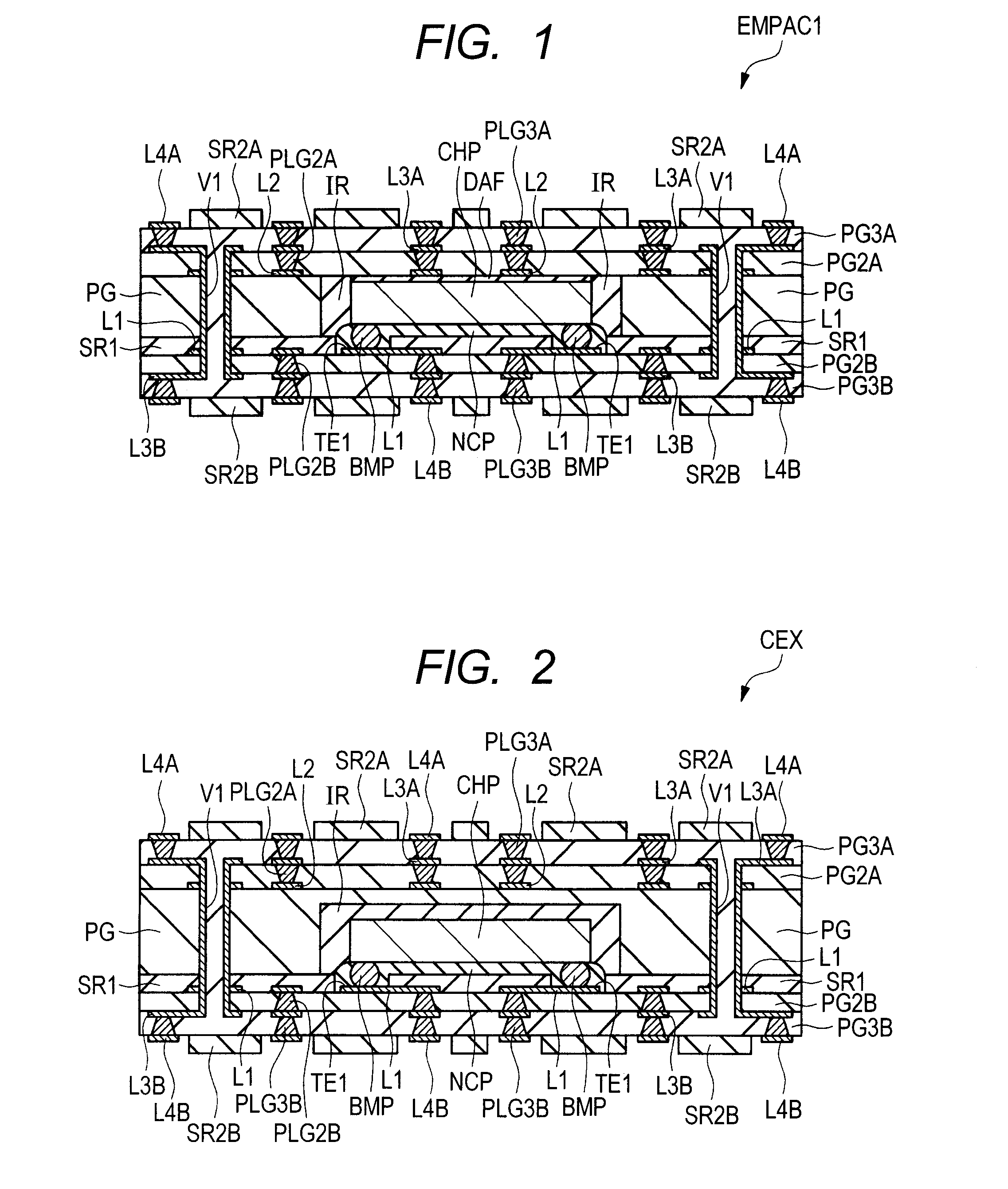
[0129]In Embodiment 3, an explanation will be given of an example in which a through via is formed with use of stud bump electrodes. FIG. 30 is a cross-sectional view showing a configuration of a chip-embedded wiring board EMPAC2 according to Embodiment 3. The configuration of the chip-embedded wiring board EMPAC2 shown in FIG. 30 is substantially the same as the configuration of the chip-embedded wiring board EMPAC1 shown in FIG. 1. That is, in the chip-embedded wiring board EMPAC2 according to Embodiment 3 also, assuming that the bump electrodes BMP are formed over the main surface (element forming surface) of the semiconductor chip CHP, the insulating film DAF is formed over the back surface (a surface on the side opposite to the main surface) of the semiconductor chip CHP. Accordingly, it becomes unnecessary to form a prepreg PG over the back surface of the semiconductor chip CHP, which brings about an effect of thinning the chip-embedded wiring board EMPAC2 in which the semicon...


PUM


Abstract

In regard to a semiconductor device having a multilayered wiring board where a semiconductor chip is embedded inside, a technology which allows the multilayered wiring board to be made thinner is provided. A feature of the present invention is that, in a semiconductor device where bump electrodes are formed over a main surface (element forming surface) of a semiconductor chip embedded in a chip-embedded wiring board, an insulating film is formed over a back surface (a surface on the side opposite to the main surface) of the semiconductor chip. As a result, it becomes unnecessary to form a prepreg over the back surface of the semiconductor chip. Therefore, an effect of thinning the chip-embedded wiring board in which the semiconductor chip is embedded is obtained.

Description

CROSS-REFERENCE TO RELATED APPLICATIONS[0001]The disclosure of Japanese Patent Application No. 2010-24097 filed on Feb. 5, 2010 including the specification, drawings and abstract is incorporated herein by reference in its entirety.BACKGROUND OF THE INVENTION[0002]The present invention relates to a semiconductor device and its manufacturing technique. In particular, it relates to a technique effectively applicable to a semiconductor device where a semiconductor chip is embedded inside a multilayered wiring board and its manufacturing technique.[0003]There is disclosed in Japanese Unexamined Patent Publication No. 2007-214535 (Patent Document 1) a technique about a printed-wiring board with a built-in semiconductor element that has excellent adhesiveness to an overlying wiring board without being affected by insufficient sealing or excessive sealing. The printed-wiring board with a built-in semiconductor element is configured so that at least the lower surface is covered with an insul...

Claims


Application Information

Patent Timeline
Patent Type & Authority Applications(United States)
IPC IPC(8): H01L23/498H01L23/552H01L21/50
CPCH01L23/3121H01L2924/1306H01L23/5389H01L23/552H01L24/81H01L25/105H01L2924/01029H01L2924/01038H01L2924/01046H01L2924/01051H01L2924/01064H01L2924/01077H01L2924/01078H01L2924/01079H01L2924/01005H01L2924/01006H01L2924/01033H01L2924/01075H01L2924/014H01L2924/13091H01L2224/45144H01L25/16H01L2225/1035H01L2225/1058H01L2224/16225H01L2224/32145H01L2224/32225H01L2224/48227H01L2224/73265H01L2924/15311H01L2924/15331H01L2924/19105H01L23/49816H01L2224/73253H01L2924/3025H01L2224/2919H01L2224/73204H01L2224/83192H01L2224/81191H01L2924/00012H01L2924/00H01L2924/181H01L24/73H01L2924/14
Inventor GOTO, MASAKATSUENOMOTO, MINORU
Owner RENESAS ELECTRONICS CORP
Why Eureka
Try Eureka