

Thin-film transistor, method of manufacturing the same, display device, and electronic apparatus
a technology of thin film transistor and display device, which is applied in the direction of transistors, semiconductor devices, electrical devices, etc., can solve the problems of reducing the storage capacity, the effect of preventing the fluctuation of the threshold voltage of the tft due to the influence of the potential of the light blocking layer, and suppressing the photo leak curren
- Summary
- Abstract
- Description
- Claims
- Application Information
AI Technical Summary
Benefits of technology
Problems solved by technology
Method used
Image

Examples
first exemplary embodiment
[0387]As a first exemplary embodiment of the present invention, an example of the structure of the thin-film transistor according to the first or second aspect of the present invention and a mode of using the thin-film transistor according to the first or second aspect of the present invention as a driving device for active matrix of a liquid crystal display device are explained in detail with reference to the drawings.
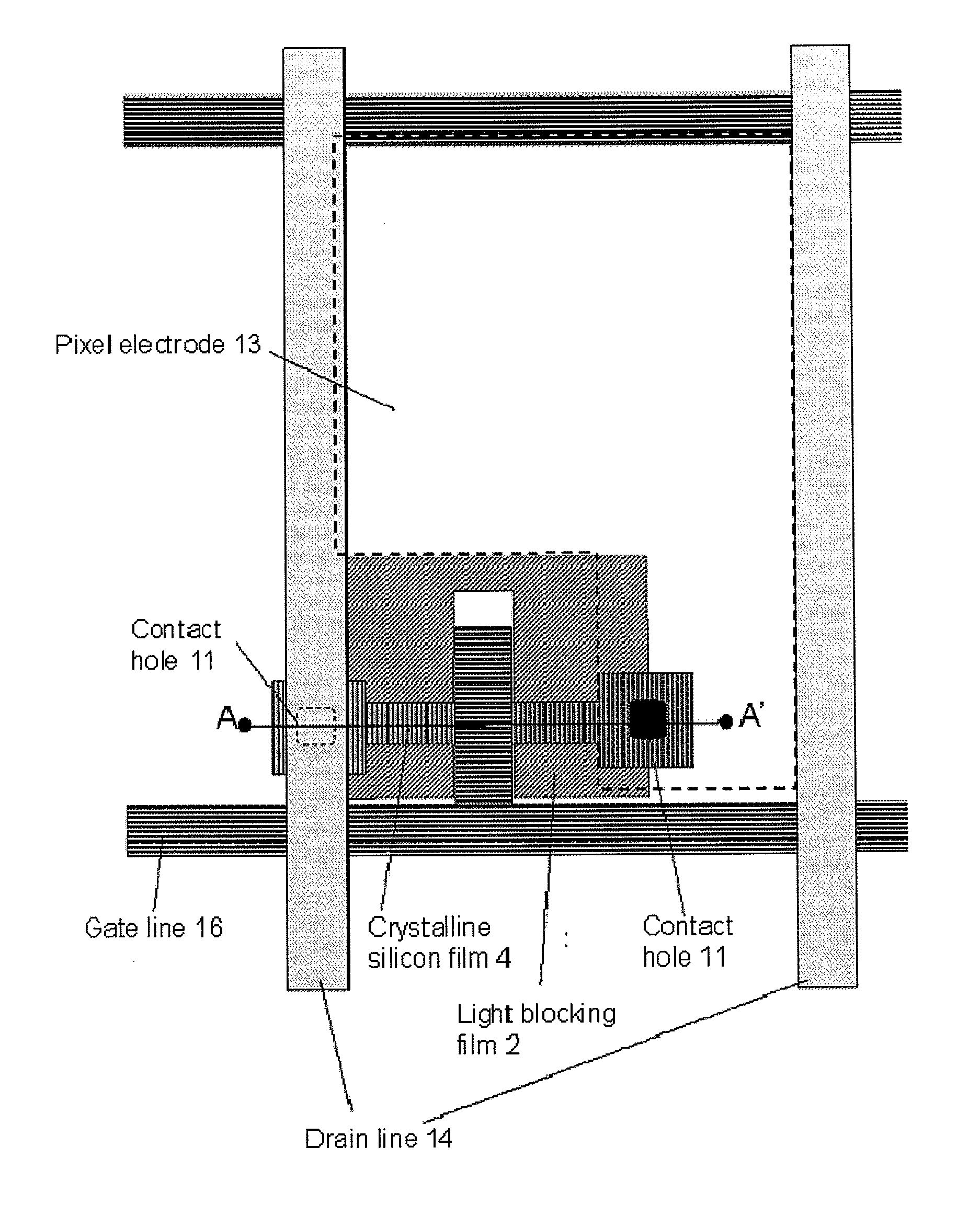
[0388]FIG. 1 is a top view schematically showing a mode of using the thin-film transistor according to the first or second aspect of the present invention as the driving device for active matrix of the liquid crystal display device. In a P-channel type TFT shown in FIG. 1, light blocking film 2 is divided into two regions across a channel region in parallel to a channel width direction. The two regions of light blocking film 2 are electrically connected by a third region provided in a region where silicon film 4 is not formed. In other words, light blocking film 2 is ...
second exemplary embodiment
[0518]As a second exemplary embodiment of the present invention, as to the method of manufacturing a thin-film transistor according to the third aspect or the fourth aspect of the present invention, by using the thin-film transistor having the structure shown in FIG. 4 according to the first exemplary embodiment of the present invention as an example, a manufacturing process of the thin-film transistor is explained in detail with reference to the drawings.
[0519]FIGS. 7-1 to 7-4 are flowcharts for illustrating a manufacturing process for the thin-film transistor according to the first exemplary embodiment of the present invention, specifically, the TFT, the sectional structure of which is shown in FIG. 3. In FIGS. 7-1 to 7-4, a series of steps comprised in the process for manufacturing a planar type TFT shown in FIG. 3; the following steps (a) to (i), excluding steps for forming second interlayer insulating film 15 and pixel electrode 13 formed on second interlayer insulating film 15...
third exemplary embodiment
[0604]As a third exemplary embodiment of the present invention, another example of the structure of the thin-film transistor according to the first aspect of the present invention and a mode of using the thin-film transistor according to the first aspect of the present invention as the driving device for active matrix of the liquid crystal display device are explained in detail with reference to the drawings.
[0605]FIG. 9 is a top view of a TFT according to the third exemplary embodiment of the present invention. As a structure shown in FIG. 9, a double gate structure in which two TFTs are connected in series between a drain region and a source region is employed. In the double gate structure, since the two TFTs are connected in series, potential (VD) of the drain region and potential (VS1) of the source region are applied to a first TFT; and potential (VD2) of the drain region and potential (VS2) of the source region are applied to a second TFT. The source region of the first TFT an...
PUM
| Property | Measurement | Unit |
|---|---|---|
| transparent | aaaaa | aaaaa |
| concentration | aaaaa | aaaaa |
| length | aaaaa | aaaaa |
Abstract
Description
Claims
Application Information