

Semiconductor light-emitting element
a technology light-emitting elements, which is applied in the direction of basic electric elements, electrical equipment, semiconductor devices, etc., can solve the problems of reducing the light extraction efficiency of elements, and achieve the effect of improving the light extraction efficiency of semiconductor light-emitting elements
- Summary
- Abstract
- Description
- Claims
- Application Information
AI Technical Summary
Benefits of technology
Problems solved by technology
Method used
Image

Examples
first embodiment
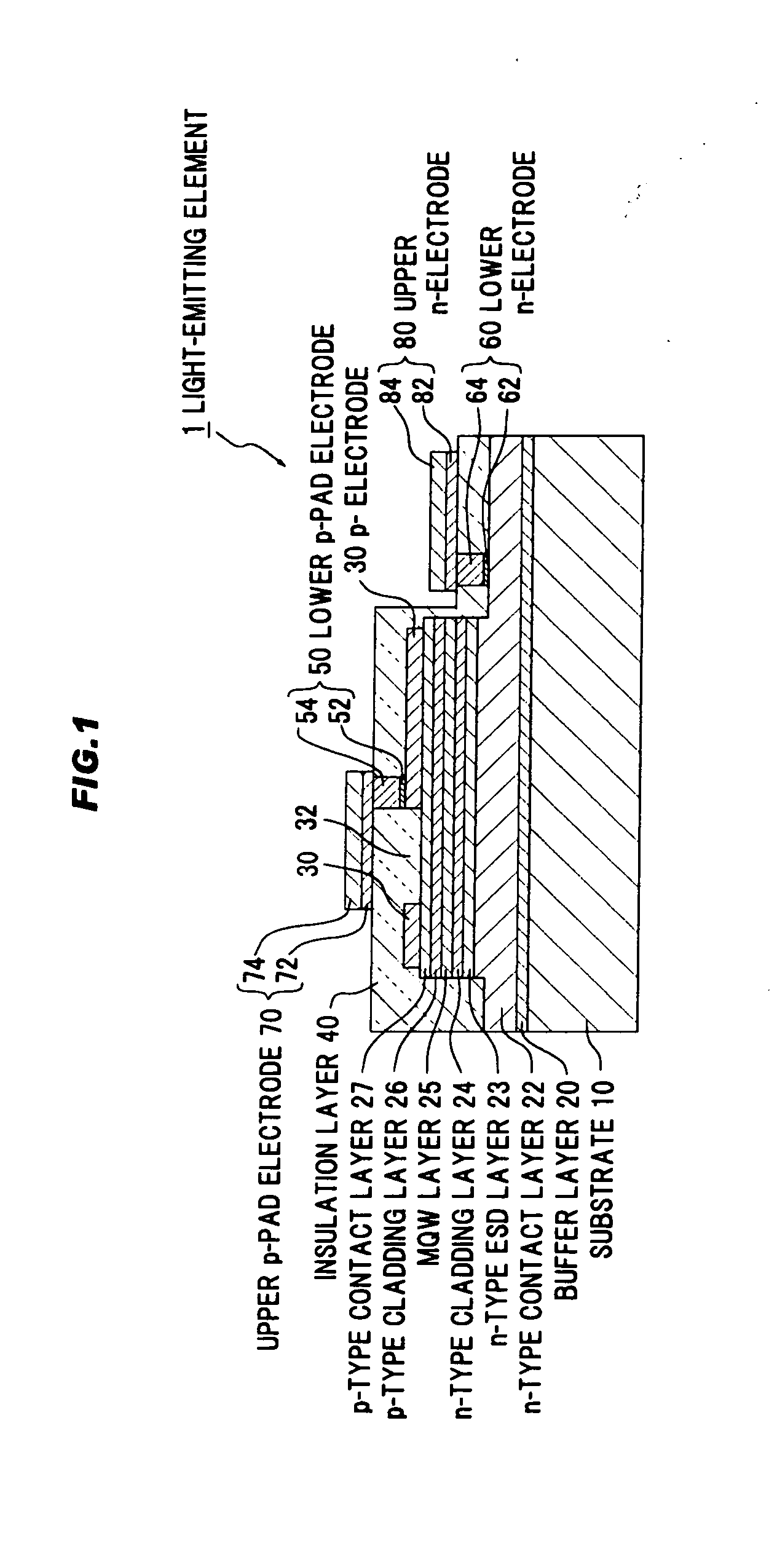
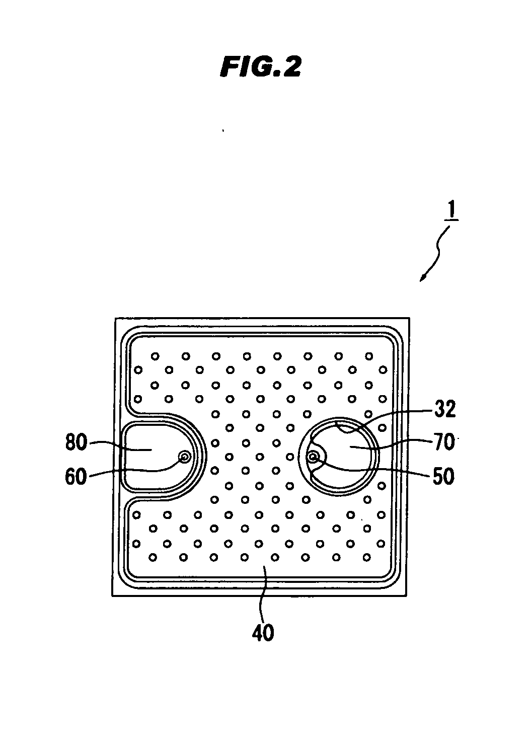
[0052]FIGS. 1 and 2 show the first embodiment of the invention. FIG. 1 is a schematic cross sectional view of a semiconductor light-emitting element.
[0053]As shown in FIG. 1, a light-emitting device 1 has a semiconductor laminated structure including a sapphire substrate 10, a buffer layer 20 provided on the sapphire substrate 10, an n-type contact layer 22 provided on the buffer layer 20, an n-type ESD layer 23 provided on the n-type contact layer 22, an n-type cladding layer 24 formed on the n-type ESD layer 23, a light-emitting layer 25 provided on the n-type cladding layer 24, a p-type cladding layer 26 provided on the light-emitting layer 25 and a p-type contact layer 27 provided on the p-type cladding layer 26. In addition, a portion of from the p-type contact layer 27 to the n-type contact layer 22 is removed by etching, thereby partially exposing the n-type contact layer 22.
[0054]Here, the buffer layer 20, the n-type contact layer 22, the n-type ESD layer 23, the n-type clad...
second embodiment
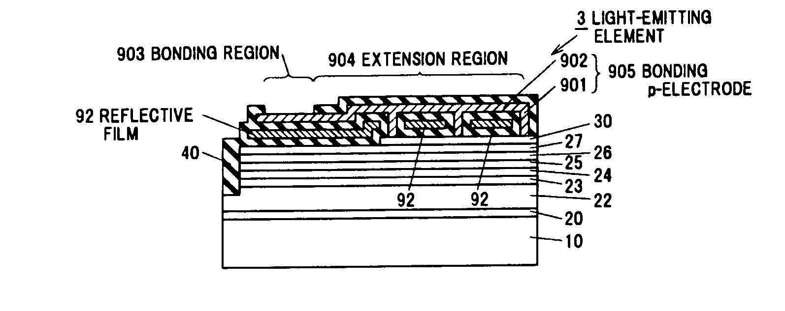
[0082]In the second embodiment of the invention, a reflective film separated from a bonding electrode is used as a reflective portion formed of a metal of which reflectance to the light emitted from the light-emitting layer 25 is high, instead of using the first metal layer 72 in the first embodiment. The explanation for the same portions as the first embodiment is omitted or simplified.
[0083]FIG. 7 is a schematic plan view of a light-emitting element 2 in a second embodiment of the invention. FIG. 8A is a vertical cross sectional view of the light-emitting element 2 taken along line A-A of FIG. 7 and FIG. 8B is a vertical cross sectional view of the light-emitting element 2 taken along line B-B of FIG. 7.
[0084]Similarly to the light-emitting element 1 in the first embodiment, the light-emitting element 2 has a semiconductor laminated structure including a sapphire substrate 10, a buffer layer 20 provided on the sapphire substrate 10, an n-type contact layer 22 provided on the buffe...
third embodiment
[0114]The third embodiment is different from the second embodiment in that a reflective portion having a high reflectance to the light emitted from the light-emitting layer 25 is provided as lower portions of a bonding p-electrode and a bonding n-electrode (the lowermost layer of a multilayer structure) instead of providing the reflective film 92. The explanation for the same portions as the second embodiment is omitted or simplified.
[0115]FIGS. 12A and 12B are vertical cross sectional views showing a light-emitting element 4 in the third embodiment. The layout of bonding p-electrodes and bonding n-electrodes is the same as that of the light-emitting element 2 in the second embodiment.
[0116]A bonding p-electrode 110 has a lower film 111 as a reflective portion and an upper film 112 thereon. A metal suitable for connection to a bonding wire, e.g., Au, is used as a material of the upper film 112. The lower film 111 is formed of a metal of which reflectance to the light emitted from th...
PUM
 Abstract
Description
Claims
Application Information