Semiconductor device

a technology of semiconductor elements and devices, applied in the direction of microstructural device assemblies, electrical transducers, electrostatic transducers of semiconductors, etc., can solve the problems of inapplicability of methods, and achieve the effects of enhancing the adhesion strength of semiconductor elements, enhancing the buffering effect of die bonding resin, and increasing the adhesion area of semiconductor elements

Active Publication Date: 2011-08-25
MMI SEMICON CO LTD
View PDF12 Cites 8 Cited by
  • Summary
  • Abstract
  • Description
  • Claims
  • Application Information

AI Technical Summary

Benefits of technology

[0011]One or more embodiments of the present invention provides a semiconductor device capable of preventing the die bonding resin from riding up the cavity through the valley section of the cavity arranged in the semiconductor element.
[0013]In a semiconductor device according to one or more embodiments of the present invention, the die bonding pad is formed so as not to contact the lower end of the valley section, and thus the die bonding resin does not touch the lower end of the valley section even if spread over the upper surface of the die bonding pad when the die bonding resin in the melted state is applied on the die bonding pad and the lower surface of the semiconductor element is overlapped thereon. Therefore, drawback in that the die bonding resin enters from the lower end of the valley section and rises up the cavity along the valley section thus fixing the diaphragm of entering the gap under the diaphragm and becoming a foreign substance can be prevented.
[0014]In a semiconductor device according to one or more embodiments the present invention, the substrate is a printed substrate, the die bonding pad is formed to include a conductor pattern of the printed substrate; and the conductor pattern is removed in a region (hereinafter referred to as valley section facing region) facing the lower end of the valley section. If the substrate is a printed substrate, an opening can be formed in the conductor pattern by removing the conductor pattern in the valley section facing region, so that the die bonding resin can be prevented from rising up along the valley section.
[0015]In a semiconductor device according to one or more embodiments of the present invention, at least one part of a surface of an outer peripheral portion of the conductor pattern removed region of the conductor pattern is formed by an inorganic material such as Cu and Au. The inorganic material particularly Cu and Au does not have satisfactory wetting property with the die bonding resin, and thus the die bonding resin flowed towards the valley section facing region can be stopped at the portion formed with the inorganic material by forming at least one part of the surface of the outer peripheral portion of the conductor pattern removed region with an inorganic material such as Cu and Au, and the die bonding resin can be prevented from flowing into the conductor pattern removing region and contacting the lower end of the valley section.
[0016]In a semiconductor device according to one or more embodiments of the present invention, an outer peripheral edge of the die bonding pad is positioned on an outer side than an outer peripheral edge of the lower surface of the semiconductor element. Accordingly the die bonding resin between the die bonding pad and the lower surface of the semiconductor element easily flows to the outer side of the semiconductor element since the die bonding pad is spread to the outer side than the semiconductor element. The die bonding resin that flows to the inner side of the semiconductor element reduces by such amount, and the die bonding resin is less likely to contact the wall surface of the cavity.
[0017]In a semiconductor device according to one or more embodiments of the present invention, the lower surface of the semiconductor element has an entire surface excluding a region in the vicinity of the lower end of the valley section adhered to the die bonding pad. Accordingly, the adhering area of the semiconductor element can be increased since the lower surface of the semiconductor element is adhered with the entire surface excluding the region in the vicinity of the lower end of the valley section, and hence the adhering strength of the semiconductor element can be enhanced and the buffering effect by the die bonding resin can be enhanced.

Problems solved by technology

These methods are thus not practical.

Method used


Image

  • Semiconductor device
  • Semiconductor device
  • Semiconductor device

Examples


first embodiment

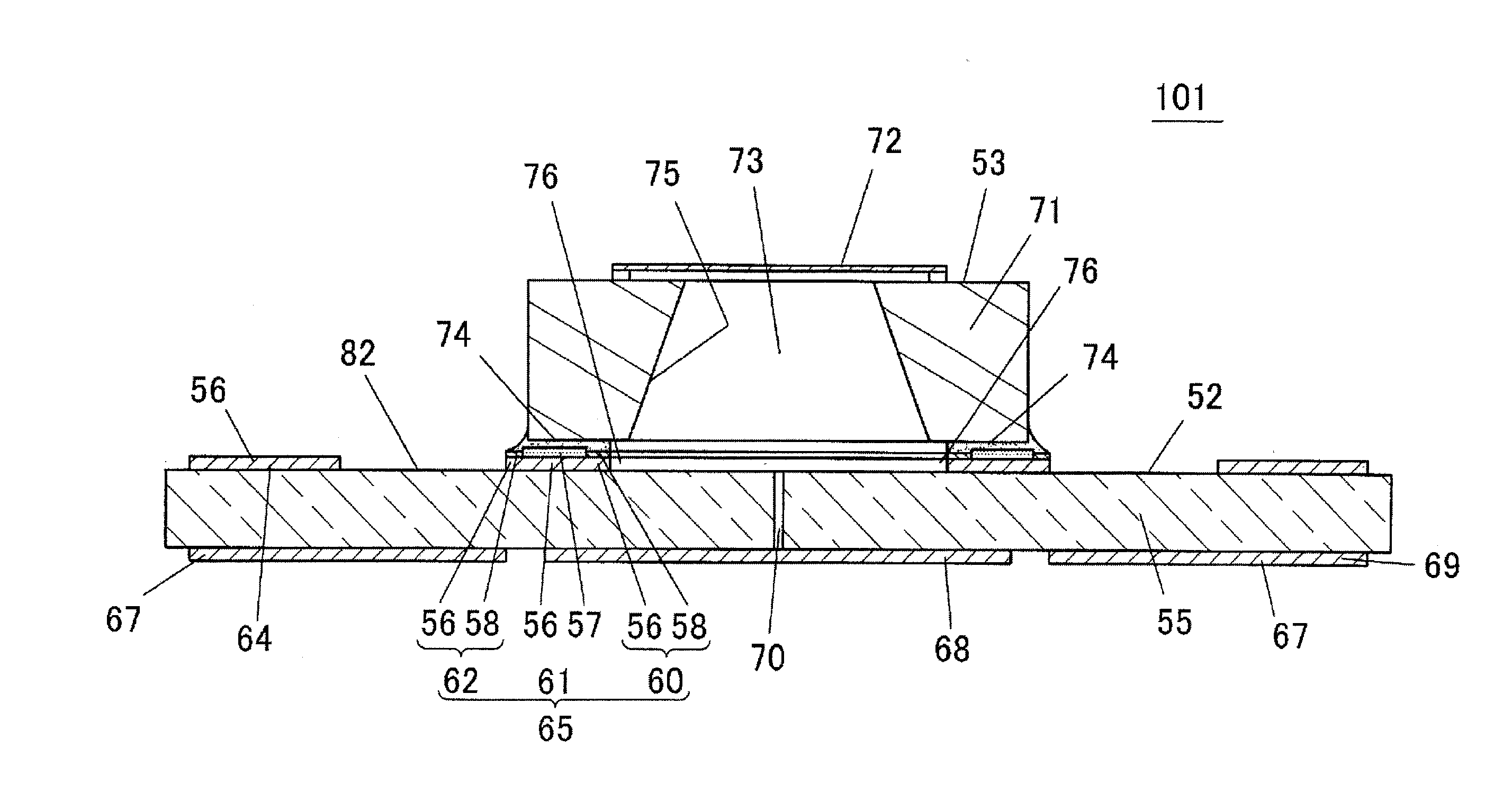
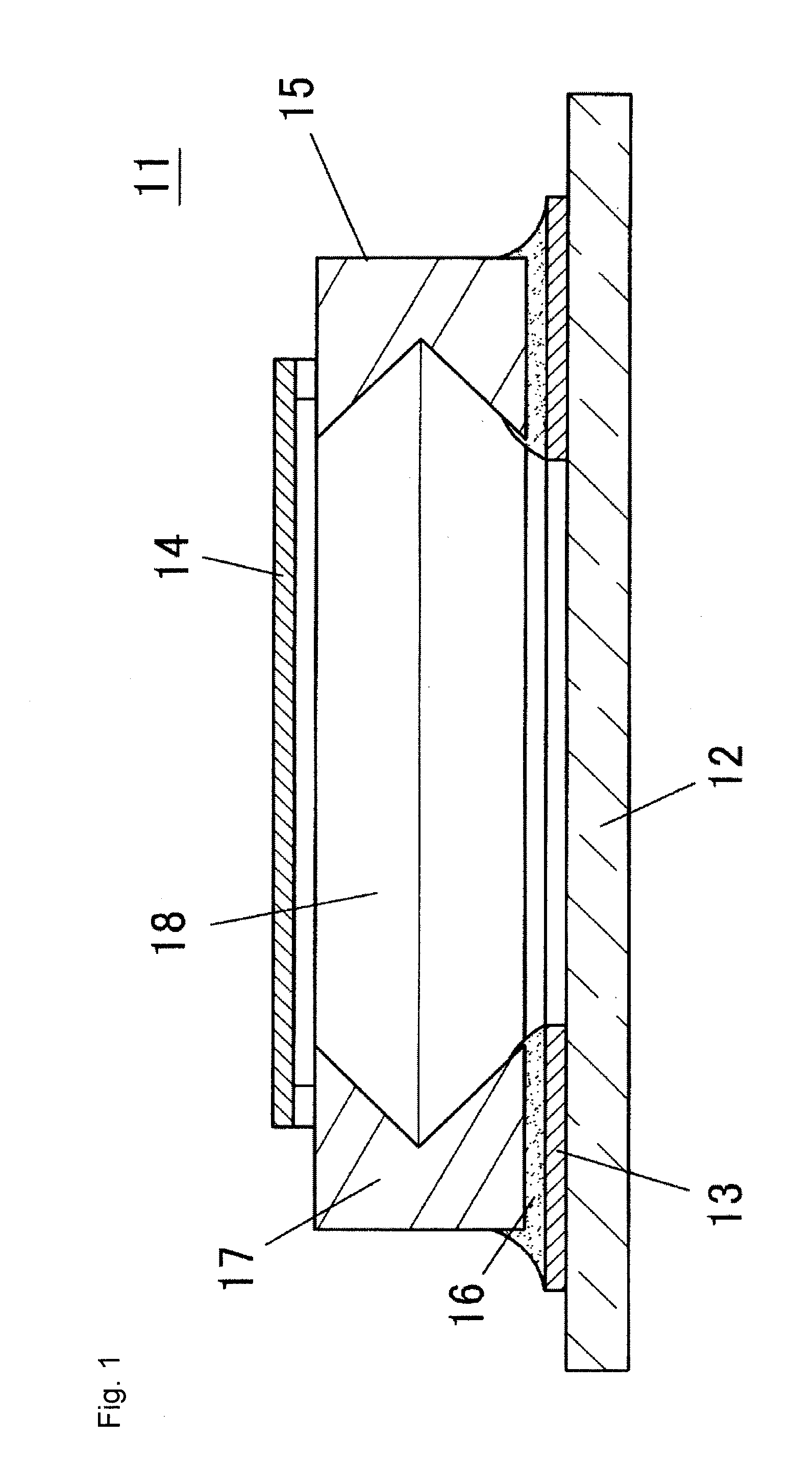
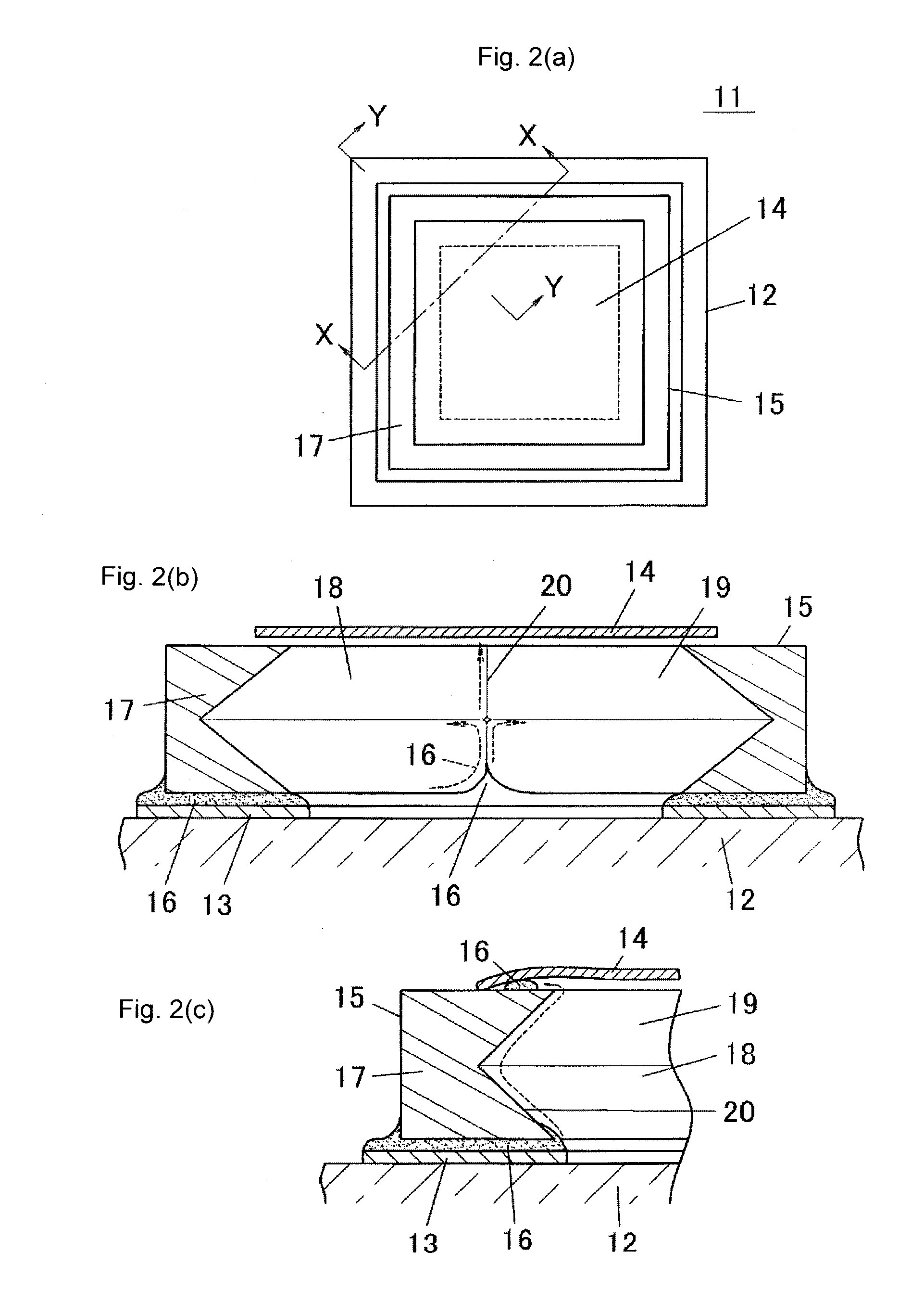
[0031]FIG. 4 is a cross-sectional view showing a structure of a semiconductor device 51 according to a first embodiment of the present invention, and shows the cross-section in the diagonal direction of a substrate 52. FIG. 5 is a plan view of the substrate 52 used in the semiconductor device 51, and also shows one part thereof in an enlarged manner. The semiconductor device 51 shown here has a semiconductor element 53 mounted on an upper surface of the substrate 52, and the semiconductor element 53 accommodated in a package (Faraday cage) including the substrate 52 and a conductive cap 54.

[0032]The substrate 52 is configured by a printed board, where a conductor pattern 56 (metal foil) of copper foil, and the like is stacked on substantially the entire surface of the upper surface of a substrate core material 55 (prepreg), as shown in FIG. 4. A conductor pattern 69 (metal foil) of Cu and the like is also stacked on substantially the entire surface of the lower surface of the substr...

second embodiment

Variant of Second Embodiment

[0058]FIG. 8 is a cross-sectional view showing a structure of a variant of the second embodiment, and shows a state before attaching the conductive cap 54. In the variant, the substrate core material 55 is omitted at the bottom surface of the opening 76 to arrange an excavated portion 83. Since the excavated portion 83 is formed in the opening 76, the depth of the opening 76 becomes deeper and the die bonding resin 74 is less likely to touch the lower end of the valley section 75 in the unlikely event the die bonding resin 74 flows into the opening 76, whereby the possibility the die bonding resin 74 runs up along the valley section 75 becomes smaller.

[0059]The deepening of the opening 76 can be applied to embodiments other than the second embodiment.

third embodiment

[0060]FIG. 9 is a cross-sectional view showing a structure of a semiconductor device 91 according to a third embodiment of the present invention, and shows a state before attaching the conductive cap 54. FIG. 10 is a plan view of the substrate 52 used in the semiconductor device 91, and also shows one part thereof in an enlarged manner. In the third embodiment, the outer peripheral side plated region 62 in the second embodiment is removed to enlarge the groove portion 82, and the outer peripheral end of the second solder resist region 61 is substantially coincided with the outer peripheral end of the lower surface of the semiconductor element 53. According to such embodiment, the die bonding resin 74 that flowed out to the outer side is less likely to flow to the ground electrode portion 64 since the groove portion 82 can be widened.


PUM


Abstract

A semiconductor device has a semiconductor element having a base, a cavity having a polygonal horizontal cross-section penetrating vertically through the base, a diaphragm arranged on the base to cover the cavity, and a substrate formed with a die bonding pad. A lower surface of the semiconductor element is adhered on the die bonding pad with a die bonding resin. The die bonding pad is formed so as not to contact a lower end of a valley section formed by an intersection of wall surfaces of an inner peripheral surface of the cavity of the semiconductor element.

Description

BACKGROUND OF THE INVENTION[0001]1. Technical Field[0002]The present invention relates to semiconductor devices. Specifically, the present invention relates to a semiconductor device in which a semiconductor element such as a sensor chip including a diaphragm is mounted on a substrate.[0003]2. Background Art[0004]FIG. 1 is a schematic cross-sectional view showing a structure of a conventional semiconductor device. A semiconductor device 11 has a lower surface of a semiconductor element 15 adhered to a die bonding pad 13 arranged on a substrate 12 like a printed wiring board using a die bonding resin 16 (silicon resin). The semiconductor element 15 has a diaphragm 14 laminated on the upper surface of a base 17, where the diaphragm 14 has the four corners fixed to the upper surface of the base 17, and a cavity 18 vertically passes through the base 17 so as not to inhibit the displacement or the vibration of the diaphragm 14. In the illustrated example, the upper half of the cavity 18 ...

Claims


Application Information

Patent Timeline
Patent Type & Authority Applications(United States)
IPC IPC(8): H01L29/84
CPCB81B2201/0257H01L2224/2731B81C3/001H01L23/552H01L2224/32225H04R19/005H04R19/04H04R31/006H01L2924/01079H01L2924/10158B81B2203/0392H01L2924/164H01L2924/16152H01L2924/00014H01L2224/83862H01L2224/83855H01L24/27H01L24/29H01L24/32H01L24/83H01L2224/2919H01L2224/73265H01L2224/83192H01L2224/83444H01L2224/83447H01L2924/0715H01L2224/48H01L2224/45099H01L23/48
Inventor ONO, KAZUYUKIMAEKAWA, TOMOFUMI
Owner MMI SEMICON CO LTD
Why Eureka
Try Eureka