Multi-gigabit millimeter wave receiver system and demodulator system

a receiver system and multi-gigabit technology, applied in phase-modulated carrier systems, amplitude demodulation, pulse techniques, etc., can solve the problem that the process of complementary metal-oxide semiconductors (cmos) cannot achieve the high transit frequency (f/sub>t) required

Active Publication Date: 2011-08-25
GEORGIA TECH RES CORP
View PDF5 Cites 80 Cited by
  • Summary
  • Abstract
  • Description
  • Claims
  • Application Information

AI Technical Summary

Benefits of technology

Briefly described, embodiments of the present invention relate to a demodulator system. Embodiments of the present inven...

Problems solved by technology

Before that time, complementary metal-oxide semiconductor (CMOS) processes could not...

Method used


Image

  • Multi-gigabit millimeter wave receiver system and demodulator system
  • Multi-gigabit millimeter wave receiver system and demodulator system
  • Multi-gigabit millimeter wave receiver system and demodulator system

Examples


Embodiment Construction

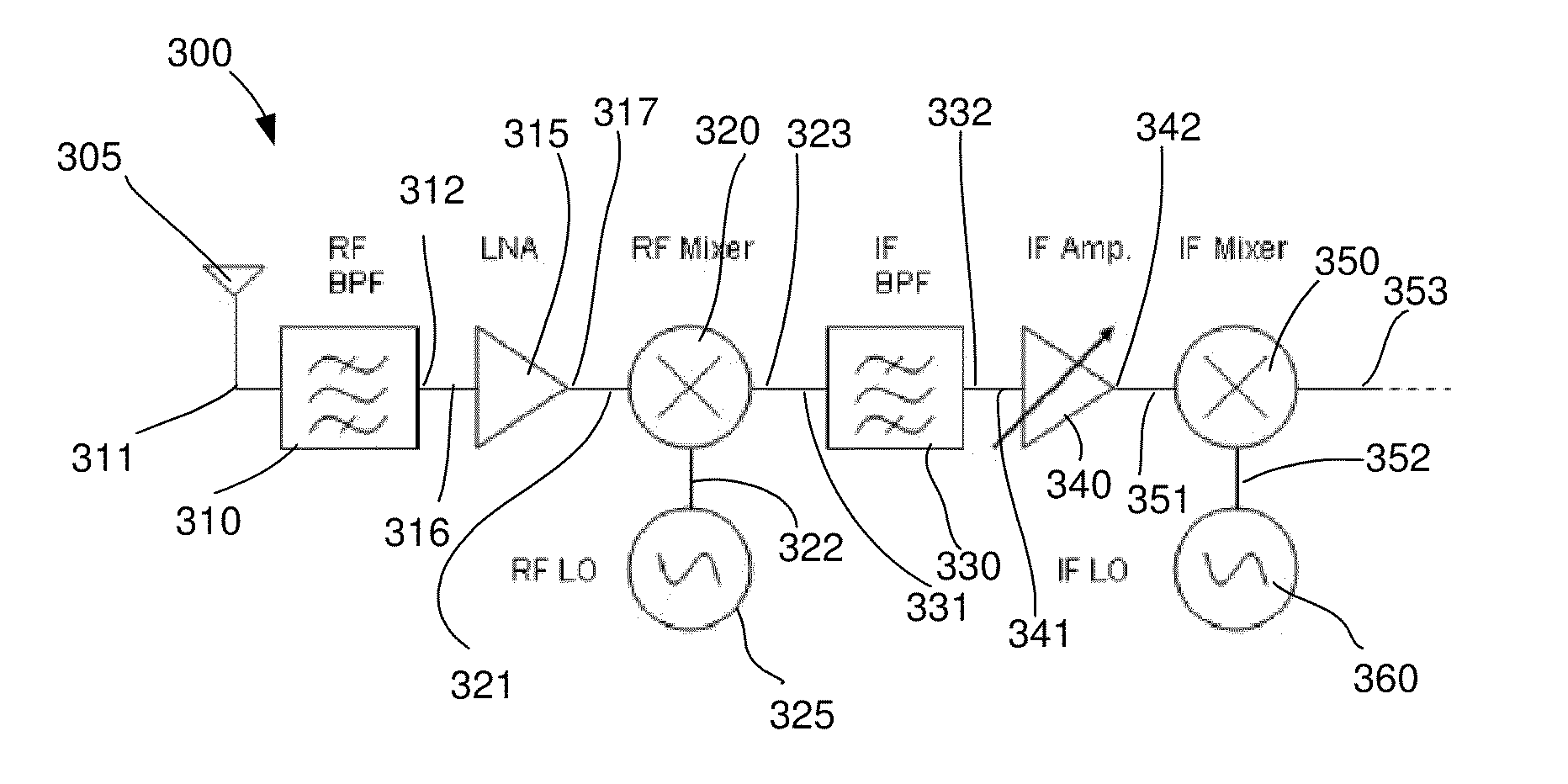
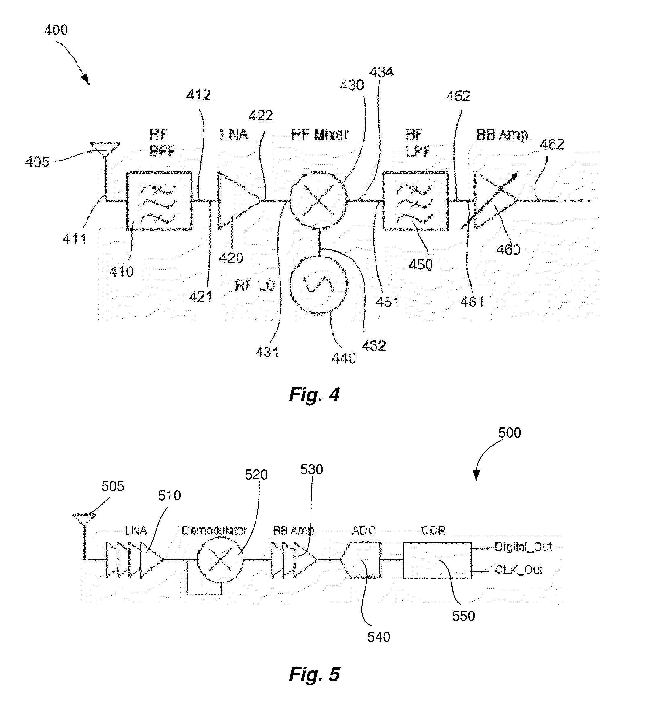
To facilitate an understanding of embodiments, principles, and features of the present invention, they are explained hereinafter with reference to implementation in illustrative embodiments. In particular, they are described in the context of being a demodulator system; other embodiments are described as a receiver system.

Embodiments of the present invention, however, are not limited to use in the described systems. Rather, embodiments of the present invention can be used to demodulate and / or receive a wireless signal.

The components described hereinafter as making up the various embodiments are intended to be illustrative and not restrictive. Many suitable components that would perform the same or a similar function as the materials described herein are intended to be embraced within the scope of embodiments of the present invention.

Referring now to the figures, wherein like reference numerals represent like parts throughout the views, embodiments of the present invention will be de...


PUM


Abstract

A receiver system and a demodulator system are configured to receive and demodulate, respectively, multi-gigabit millimeter wave signals being wirelessly transmitted in the unlicensed wireless band near 60 GHz.

Description

BACKGROUNDUp until the mid-1990s the wireless communication market was dominated by designs in the III-V semiconductor processes, such as Gallium Arsenide (GaAs) or silicon bipolar technologies. Before that time, complementary metal-oxide semiconductor (CMOS) processes could not achieve the high transit frequencies (fT) required at transmitter / transceiver front ends. But CMOS was and continues to be the clear choice for implementing digital circuits, as it is the lowest cost, high-volume semiconductor fabrication technology available.Driven by the prospects of lower cost designs through increased integration of analog and digital content on the same chip and the replacement of expensive GaAs front end circuitry with less expensive CMOS implementations, the development of RF CMOS received a great deal of attention.For example, FIG. 1 illustrates a diagram of conventional transit frequencies for CMOS and Silicon Germanium (SiGe) processes at different technology nodes. Notably, the 90...

Claims


Application Information

Patent Timeline
IPC IPC(8): H04W88/02
CPCH03D7/125H04B1/16H04B1/30H03D2200/0074
Inventor JUNTUNEN, ERICPINEL, STEPHANELASKAR, JOYYEH, DAVIDSARKAR, SAIKAT
Owner GEORGIA TECH RES CORP
Why Eureka
Try Eureka