
Integrated magnetic sensor for detecting horizontal magnetic fields and manufacturing process thereof

a technology of horizontal magnetic field and integrated magnetic sensor, which is applied in the direction of magnetic sensor packaging, magnetic sensor geometrical arrangement, single device manufacturing, etc., can solve the problems of high cost, failure of electronic components associated with the sensor, and the proximity of magnetic core or concentrator to the sensitive elemen

Active Publication Date: 2011-09-01
STMICROELECTRONICS SRL
View PDF15 Cites 39 Cited by
  • Summary
  • Abstract
  • Description
  • Claims
  • Application Information

AI Technical Summary

Benefits of technology

[0014]One embodiment is a magnetic sensor of the type indi...

Problems solved by technology

On the other hand, providing the magnetic core or concentrator in proximity of the sensitive element is problematical.
In fact, ferromagnetic materials generally contain iron, nickel, cobalt, and other contaminating elements that in some cases may lead to failure of the electronic components associated with the sensor.
The greater the number of technological steps executed after deposition of the ferromagnetic material, the greater the number of apparatuses that are used only to process the wafers with magnetic sensors and the higher the costs.
The problems referred to above are all the more serious when the associated read circuit is integrated with the sensor: for example, it would be necessary to have particularly thick oxide layers causing the manufacture of deep vias to be particularly complex on account of the high aspect ratio.
In addition, since the ferromagnetic layer generally has a wide area, problems may arise also in positioning the vias.
For these reasons, it would be desirable to be able to form the ferromagnetic layer at the end of the manufacturing process, immediately prior to passivation and opening of the pads, but this technological requirement conflicts with the obtaining a high sensitivity.

Method used


Image

  • Integrated magnetic sensor for detecting horizontal magnetic fields and manufacturing process thereof
  • Integrated magnetic sensor for detecting horizontal magnetic fields and manufacturing process thereof
  • Integrated magnetic sensor for detecting horizontal magnetic fields and manufacturing process thereof

Examples


Embodiment Construction

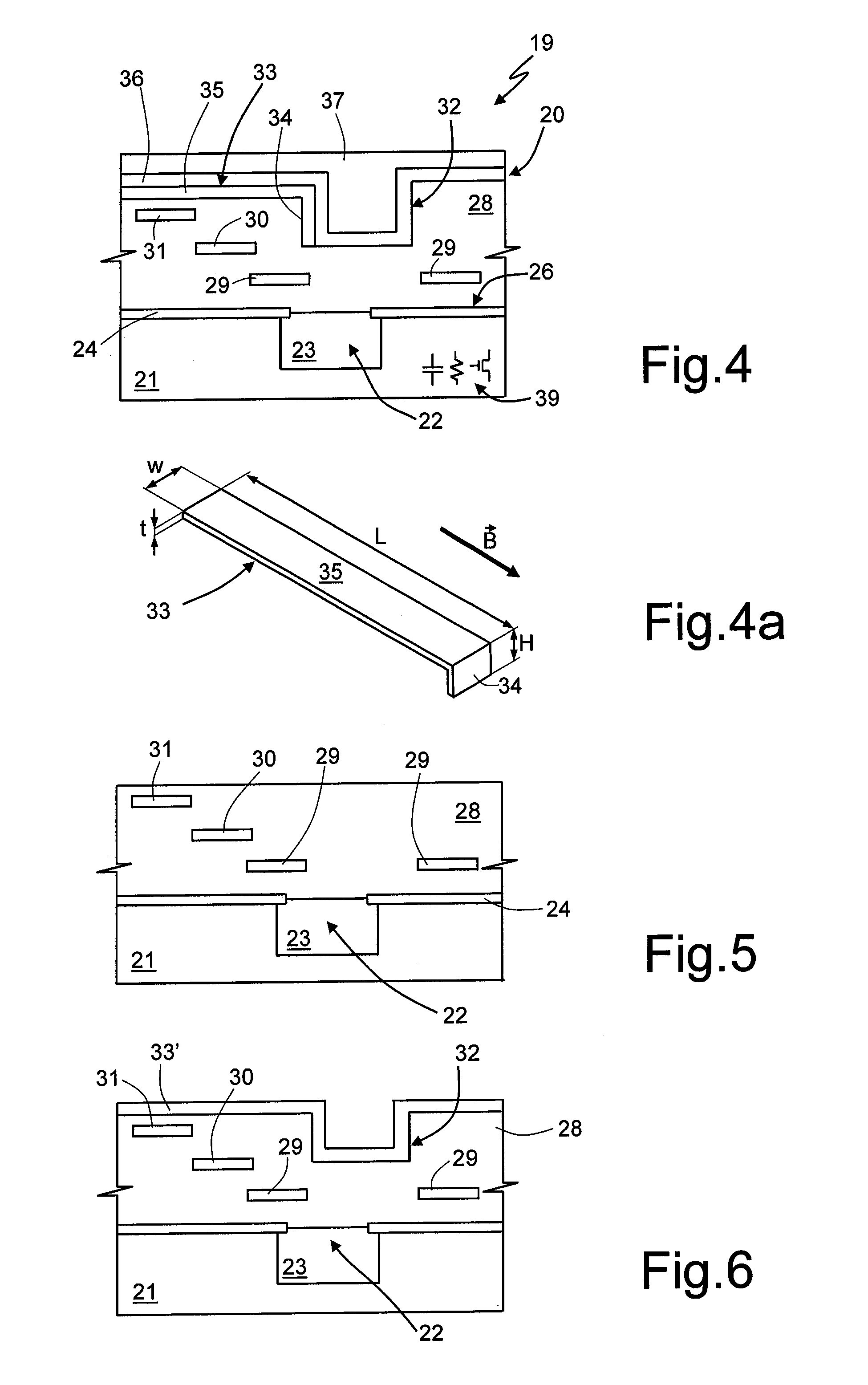
[0031]FIG. 4 shows an embodiment of a Hall-effect sensor 19 having a non-planar concentrator.

[0032]In detail, a chip 20 comprises a substrate 21 of semiconductor material, for example silicon, which accommodates a Hall cell 22 formed in an active area 23. The active area 23, for example a N-type region, is here delimited by a field-insulation region 24 of silicon oxide. Pairs of conductive biasing and sensing regions are formed, in a per se known manner, in areas arranged in front of and behind the drawing plane (and thus not visible).

[0033]A dielectric layer 28, for example an oxide layer typically made up of a plurality of superimposed layers, covers the surface 25 of the substrate 21 and accommodates various metallization levels. Visible in the example shown are first metallization regions 29, formed in a first metallization layer, a second metallization region 30, formed in a second metallization layer, and a third metallization region 31, formed in a third metallization layer. ...


PUM

PropertyMeasurementUnit
Thicknessaaaaaaaaaa
Magnetic fieldaaaaaaaaaa
Heightaaaaaaaaaa

Abstract

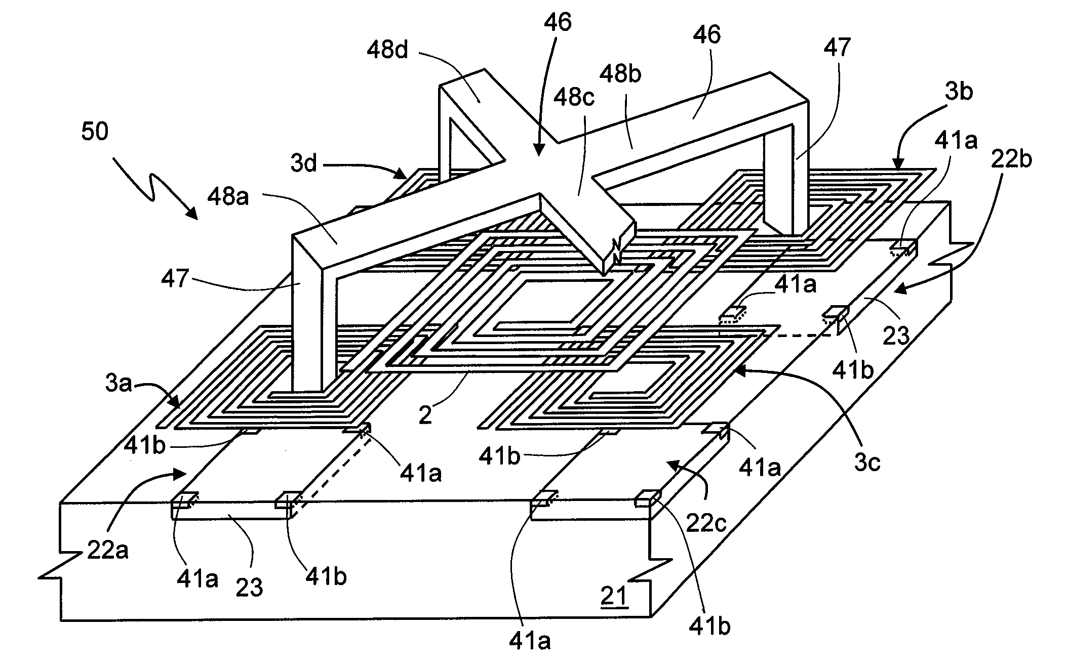
The integrated magnetic sensor for detecting an external magnetic field, is formed by a body of semiconductor material having a surface; an insulating layer covering the body of semiconductor material; a magnetically sensitive region, for example a Hall cell, extending inside the body; and a concentrator of ferromagnetic material, extending on the Hall cell and having a planar portion extending parallel to the surface of the substrate on the insulating layer. The concentrator terminates with a tip protruding peripherally from, and transversely to, the planar portion toward the Hall cell. When the magnetically sensitive region is a sensing coil of a fluxgate sensor, it is formed on the substrate, embedded in the insulating layer, and the tip of the concentrator can reach as far as the sensing coil.

Description

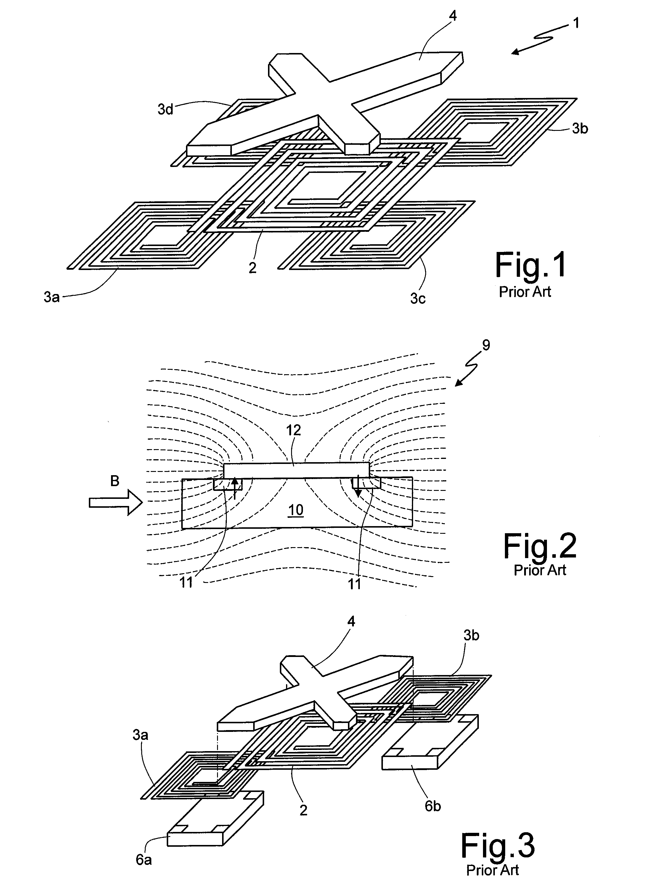
BACKGROUND[0001]1. Technical Field[0002]The present disclosure relates to an integrated magnetic sensor for detecting horizontal magnetic fields and manufacturing process thereof. In particular, the disclosure regards an integrated magnetic sensor provided with a magnetic concentrator.[0003]2. Description of the Related Art[0004]As is known, the integration of a thin ferromagnetic layer in a standard CMOS or CMOS-compatible process enables provision of integrated magnetic-field sensors, such as fluxgate sensors and Hall-effect sensors, capable of detecting horizontal magnetic fields.[0005]An example of a fluxgate sensor of a planar type sensitive to external magnetic fields parallel to the surface of a chip is described in U.S. Pat. No. 6,404,192 and shown in FIG. 1. The sensor 1 comprises a magnetic core 4, here cross-like shaped, overlying an exciting coil 2, which in turn overlies four sensing coils 3a, 3b, 3c and 3d, arranged on a substrate (not shown). By supplying the exciting...

Claims


Application Information

Patent Timeline
IPC IPC(8): G01B7/30G01R33/02G01R33/06H01L21/00
CPCY10T29/41G01R33/0005G01R33/0052G01R33/0047G01R33/072G01R33/04
Inventor PACI, DARIOIULIANO, PAOLORIVA, CATERINAMORELLI, MARCO
Owner STMICROELECTRONICS SRL
Learn More