Layered structure and piezoelectric device using the same

a piezoelectric device and layer structure technology, applied in the field of layer structure, can solve the problems of little progress, adhesive hinders the favorable contact between the piezoelectric film and the electrode, and the device is flexible, and achieves excellent piezoelectric performance, high reliability of the piezoelectric device, and excellent piezoelectric performan

Active Publication Date: 2011-09-08
FUJIFILM CORP
View PDF10 Cites 29 Cited by
  • Summary
  • Abstract
  • Description
  • Claims
  • Application Information

AI Technical Summary

Benefits of technology

[0026]The layered structure of the present invention includes a composite piezoelectric film formed on a resin substrate and constituted by an organic polymer resin matrix and a plurality of inorganic piezoelectric bodies dispersed in the matrix. As such configuration includes, as the piezoelectric film, a composite piezoelectric film constituted by a flexible organic polymer resin and inorganic piezoelectric bodies that show an excellent piezoelectric performance dispersed in the resin, the layered structure of the present invention may provide a flexible piezoelectric device with an excellent piezoelectric performance.
[0027]Further, the layered structure of the present invention may be obtained by forming a piezoelectric film on a resin substrate without using an adhesive, and each of the substrate and piezoelectric film include a resin, so that detachment or cracking due to an external force, such as bending, is unlikely to occur in the piezoelectric film. Consequently, the layered structure of the present invention may provide a highly reliable piezoelectric device.
[0028]Still further, when a configuration is adopted in which a photosensitive resin, such as a photoresist resin, is used as the organic polymer resin, high definition patterning can be achieved. Thus, in the manufacture of an arrayed device, such as a sensor array or the like, a high definition array can be realized, whereby a high performance flexible arrayed piezoelectric device with little cross-talk may be provided. Further, in the case of a configuration in which a piezoelectric body formed of a pervskite oxide (which may include an unavoidable impurity) having a composition represented by General Formula (PX) above is used, as the inorganic piezoelectric body, a non-lead based flexible piezoelectric device excellent in piezoelectric performance and thermal stability at room temperature may be provided.

Problems solved by technology

Whereas the flexibilization in the field of displays and electronic papers in wearable and ambient device configurations is moving forward steadily, the flexibilization of devices that use a piezoelectric material, such as various types of sensors, actuators, memories, and the like, is making little progress due to the fact that high temperature film forming of 600° C. or more is generally required for the manufacture of an inorganic piezoelectric material having excellent piezoelectricity and thereby a high heatproof temperature is required for the flexible substrates.
The piezoelectric polymers, however, have a small piezoelectric d constant in comparison with inorganic piezoelectric materials, and therefore, they are limited to certain applications, such as pressure sensors and the like, that do not require a high piezoelectric performance.
As a thin film piezoelectric material having a lower electrode layer formed on the bonding surface with a flexible substrate is actually used, the bonding using an adhesive may possibly result in that the adhesive hinders favorable contact between the piezoelectric film and electrode.
Where the flexible substrate is a resin substrate, the piezoelectric film can not follow the deformation of the substrate due to differences in the rigidity and modulus of elasticity, whereby the piezoelectric film may have a crack or the piezoelectric film may be peeled off due to detachment of the adhesive.

Method used


Image

  • Layered structure and piezoelectric device using the same
  • Layered structure and piezoelectric device using the same
  • Layered structure and piezoelectric device using the same

Examples


example 1

[0098]First, as basic ingredients, BaTiO3, Bi2O3, and Fe2O3 were blended to obtain a composition of (Ba0.2, Bi0.8) (Ti0.2, Fe0.80)O3. At that time, Bi2O3 was in excess by 0.5 mol %. The blended raw material powder was wet mixed in ethanol by a ball mill to prepare a mixed powder. After mixing, the mixed powder was shaped by drying and subjected to calcination at 750° C. for three hours. Thereafter, it is crushed and subjected to press molding.

[0099]The obtained compact was baked at 930° C. for ten hours, then crushed, and screened by a 400 mesh (μm) screen to obtain piezoelectric ceramics powder. The composition of the obtained powder was measured by ICP and it was confirmed to be the target composition. Also, it was confirmed that the obtained powder has a perovskite single phase (FIG. 6).

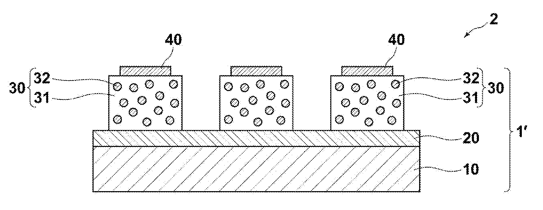
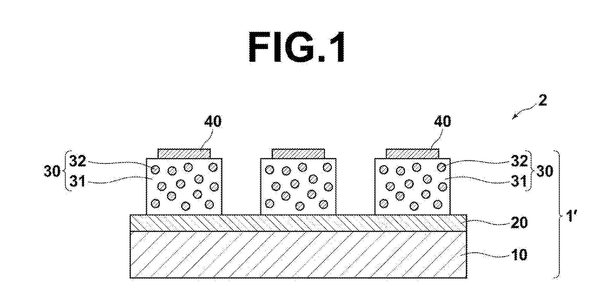
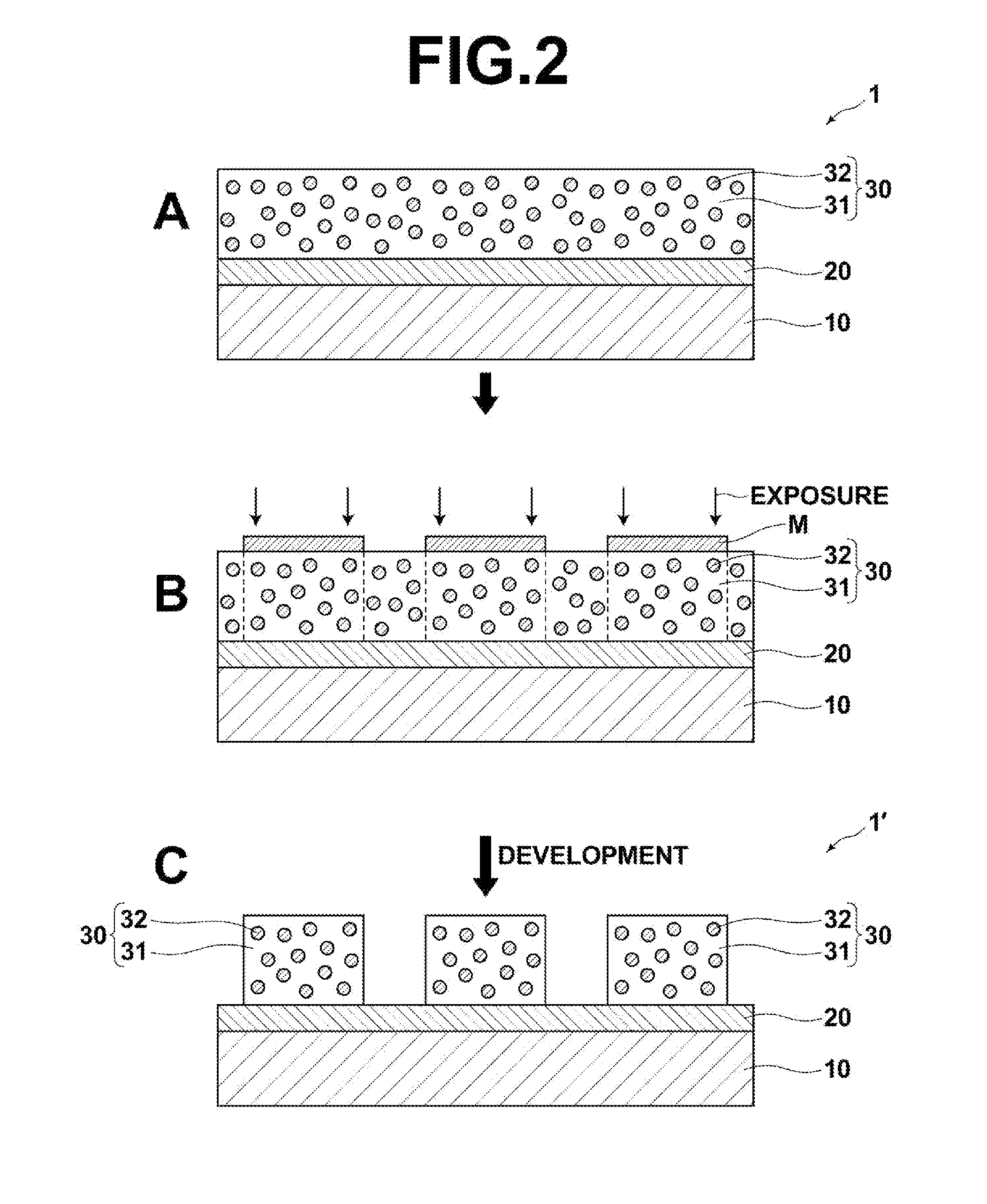
[0100]Then, SU-8 negative type resist was provided and the obtained ceramics powder was added to the resist by about 50 vol. %, which was then sufficiently mixed by a mixing mill. The obtained mix...


PUM

PropertyMeasurementUnit
temperatureaaaaaaaaaa
piezoelectricaaaaaaaaaa
photosensitivityaaaaaaaaaa

Abstract

A layered structure, including a flexible resin substrate and a composite piezoelectric film formed on the resin substrate and constituted by an organic polymer resin matrix and a plurality of inorganic piezoelectric bodies dispersed in the matrix.

Description

BACKGROUND OF THE INVENTION[0001]1. Field of the Invention[0002]The present invention relates to a layered structure suitable for use with sensor arrays a piezoelectric body, such as infrared sensors, ultrasonic sensors, and pressure sensors, actuator arrays, patterned memories, and the like. The invention also relates to a piezoelectric device using the layered structure.[0003]2. Description of the Related Art[0004]For I / O devices, small and light weight wearable devices are desired for portable use and ambient devices that fit in the environment are desired for stationary use in order to achieve the goal of realizing a ubiquitous society. From the viewpoint of ease of use and safety, it is important that these devices are “light weighted, not easily broken, and flexible”. Consequently, a trend towards flexibilization in various devices has recently been accelerated.[0005]Whereas the flexibilization in the field of displays and electronic papers in wearable and ambient device confi...

Claims


Application Information

Patent Timeline
Patent Type & Authority Applications(United States)
IPC IPC(8): B32B3/10G03F7/20B32B9/00H01L41/45
CPCB32B9/00B32B3/10G03F7/20H01L41/45Y10T428/24612Y10T428/24893Y10T428/24851Y10T428/24909Y10T428/24802H10N30/10513H10N30/852H10N30/082H10N30/092H10N30/098
Inventor SAKASHITA, YUKIO
Owner FUJIFILM CORP
Why Eureka
Try Eureka