Multilayer reflective film coated substrate, reflective mask blank, and method of manufacturing a reflective mask

a reflective film and substrate technology, applied in the field of multi-layer reflective film coated substrates, reflective mask blanks, and manufacturing methods, can solve the problems of difficult to avoid m, low position accuracy, and remarkable photolithography process used in semiconductor manufacturing processes, etc., to achieve accurate avoidance, high accuracy, and sufficient contrast

Active Publication Date: 2011-09-08
HOYA CORP
View PDF3 Cites 8 Cited by
  • Summary
  • Abstract
  • Description
  • Claims
  • Application Information

AI Technical Summary

Benefits of technology

[0019]According to a multilayer reflective film coated substrate of this invention, by forming, on a main surface of a substrate, a reference point mark in the form of a recess having a depth of 10 μm or more and a width of 80 μm or more and having a cross-sectional shape in which the width decreases from the main surface toward a bottom of the recess, even if a multilayer reflective film is formed over the reference point mark, sufficient contrast for inspection light for defect inspection is obtained so that a position of the reference point mark can be identified with high accuracy. As a consequence, there is obtained the multilayer reflective film coated substrate that can specify a position of a defect with an accuracy on the order of μm using the reference point mark as a reference. Further, even in the case where a reflective mask blank is manufactured by forming an absorber film and so on an upper surface of this multilayer reflective film coated substrate, sufficient contrast can be obtained between the reference point mark and its peripheral portion even by irradiating the inspection light onto the absorber film. Since the position of the defect can be specified with the accuracy on the order of μm, the defect can be accurately avoided upon patterning the absorber film into a transfer pattern so that it is possible to manufacture a reflective mask with high accuracy.

Problems solved by technology

On the other hand, with the increasing demand for miniaturization in the photolithography process, problems in the photolithography process used in the semiconductor manufacturing processes are becoming remarkable.
As one of them, there is cited a problem of a defect of a photomask substrate formed with a pattern, which is used in the photolithography process.
As a consequence, the positional accuracy is low and thus, when patterning a light-shielding film while avoiding the defect, it is difficult to avoid it on the order of μm.

Method used


Image

  • Multilayer reflective film coated substrate, reflective mask blank, and method of manufacturing a reflective mask
  • Multilayer reflective film coated substrate, reflective mask blank, and method of manufacturing a reflective mask
  • Multilayer reflective film coated substrate, reflective mask blank, and method of manufacturing a reflective mask

Examples


examples 1 to 5

[0034]Hereinbelow, as Examples 1 to 5, there are shown the results of manufacturing reflective mask blanks each using a glass substrate having a reference point mark of the shape shown in FIG. 2 and examining whether identification of each reference point mark is good or bad.

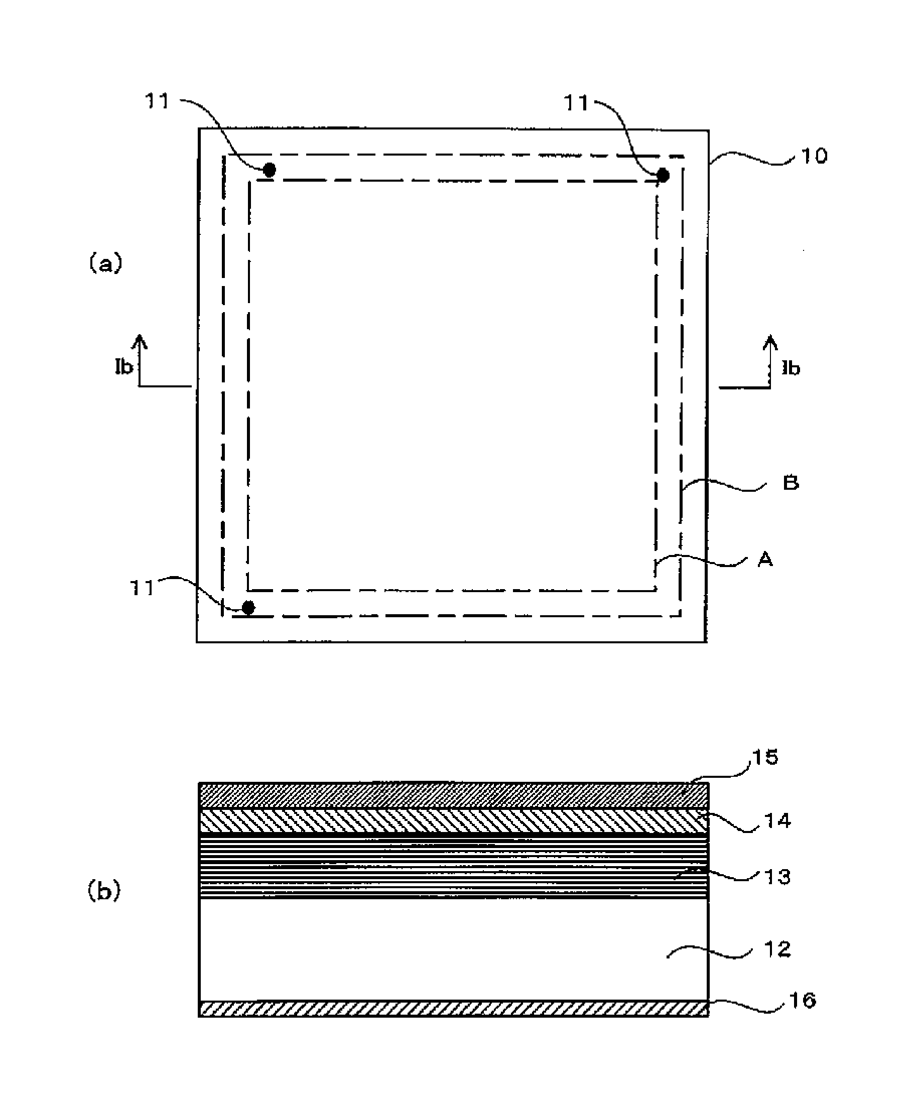
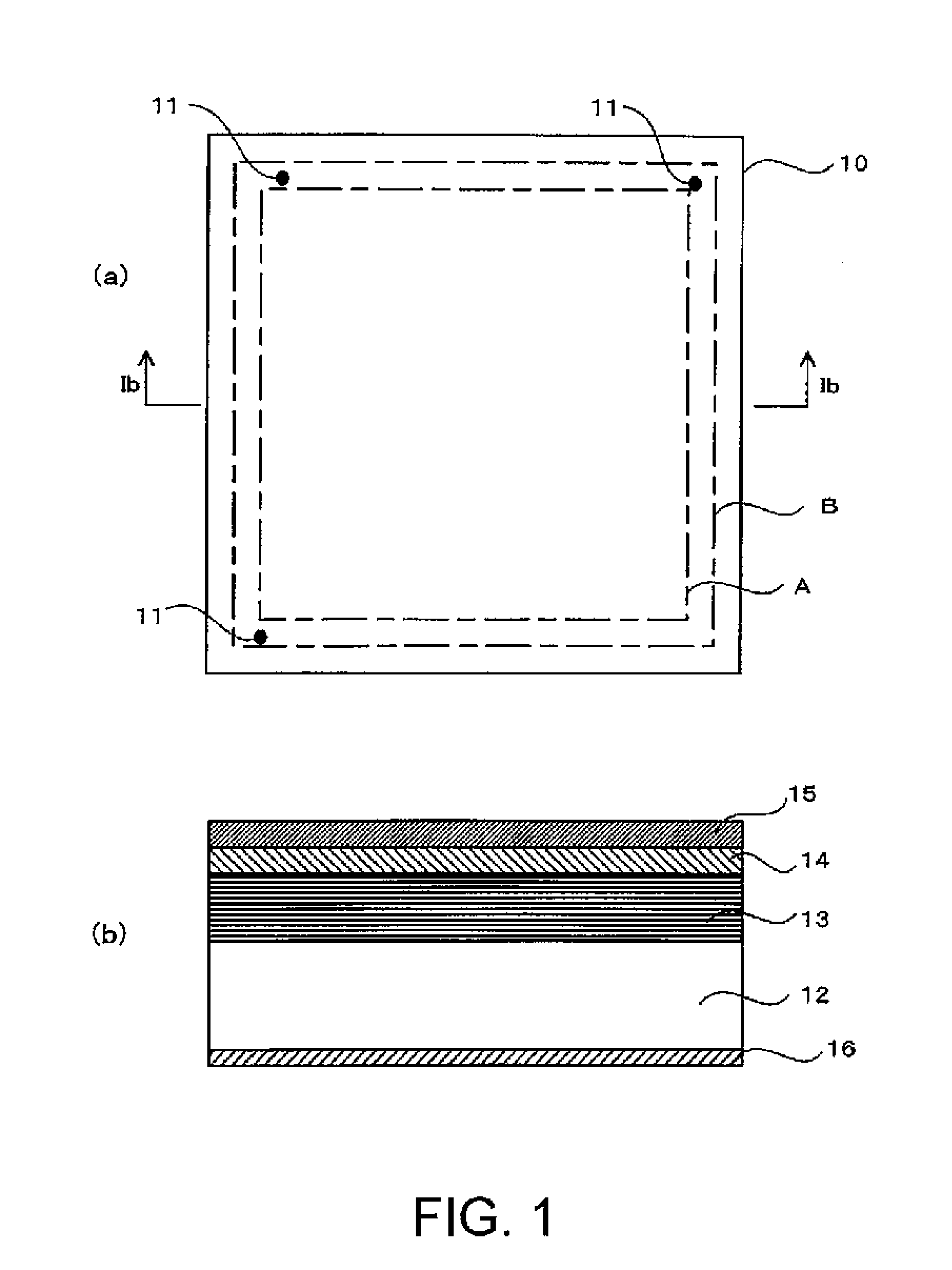
[0035]First, a glass substrate of 6-inch square (152.4 mm×152.4 mm×6.35 mm) was used as a substrate and a reference point mark was formed in an area outside of a 132 mm square area (this area is a transfer pattern area) with respect to the center of a substrate main surface and inside of a 142 mm square area. This is because the area inside of 132 mm square is an area where a transfer pattern is to be formed, while, in the area outside of 142 mm square, the flatness is not good so that there is a possibility of the occurrence of position offset or the like upon forming the reference point mark.

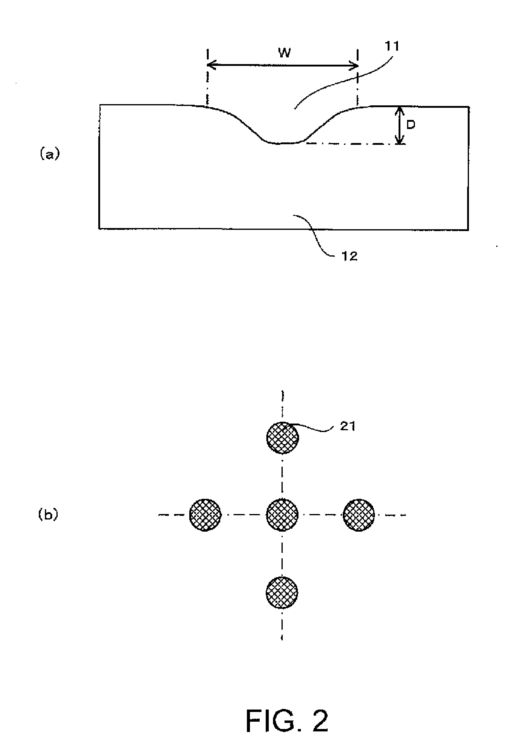
[0036]As the reference point mark, a recess was formed using the carbon dioxide laser described above. By changing the i...


PUM

PropertyMeasurementUnit
depthaaaaaaaaaa
depthaaaaaaaaaa
wavelengthaaaaaaaaaa

Abstract

Provided is a reflective mask blank, wherein even if inspection light for defect inspection is irradiated onto an uppermost surface of a multilayer reflective film or of an absorber film formed over a reference point mark, sufficient contrast is obtained between a position of the reference point mark and its peripheral portion so that the position of the reference point mark can be identified with high accuracy. By forming a reference point mark (11) in the form of a recess having a depth of 10 μm or more and a width of 80 μm or more on a main surface of a substrate (12), even if a multilayer reflective film (13), an absorber film (15), and so on are formed over the reference point mark (11), sufficient contrast for the inspection light is obtained so that the position of the reference point mark (11) can be identified with high accuracy.

Description

TECHNICAL FIELD[0001]This invention relates to a multilayer reflective film coated substrate, a reflective mask blank, and a method of manufacturing a reflective mask.BACKGROUND ART[0002]In recent years, with higher integration of semiconductor devices, patterns finer than the transfer limit of the photolithography technique using the conventional ultraviolet light have been required in the semiconductor industry. In order to enable transfer of such fine patterns, the EUV lithography being an exposure technique using extreme ultraviolet light (hereinafter referred to as EUV light) with a shorter wavelength is expected to be promising. Herein, the EUV light represents light in a wavelength band of the soft X-ray region or the vacuum ultraviolet region and, specifically, light having a wavelength of about 0.2 nm to 100 nm.[0003]As an exposure mask for use in this EUV lithography, use is normally made of a reflective mask in which a multilayer reflective film (multilayer film) for refl...

Claims


Application Information

Patent Timeline
Patent Type & Authority Applications(United States)
IPC IPC(8): G03F1/00G03F1/24
CPCG03F1/24G03F1/62G03F1/86H01L21/0274H01L21/0337
Inventor SHOKI, TSUTOMU
Owner HOYA CORP
Why Eureka
Try Eureka