
Semiconductor integrated circuit

a technology of integrated circuits and semiconductors, applied in the direction of fault response, redundant data error correction, instruments, etc., can solve the problems of inability to monitor for errors at all times, failure to perform error correction, and malfunction of digital circuits, etc., to achieve the effect of improving reliability

Active Publication Date: 2011-09-08
RENESAS ELECTRONICS CORP
View PDF6 Cites 16 Cited by
  • Summary
  • Abstract
  • Description
  • Claims
  • Application Information

AI Technical Summary

Benefits of technology

[0031]According to the present invention, it is possible to provide a semiconductor integrated circuit with enhanced reliability.

Problems solved by technology

One of the causes inducing a digital circuit malfunction is a soft error.
However, in a rectification method when an error occurs, according to Japanese Application Publication No. 2004-38468, error rectification is performed only at timing when data is read from or written into the memories.
Therefore, there is a problem in which monitoring for error occurrence at all times is impossible.
Consequently, if a hard error has occurred in the three memories due to a physical factor, mismatch between data and its redundant data always occurs in each memory and a loop of rewriting to the memories takes place.
Although an error, whenever occurred, is logged in a history file on the server, what factor causes the error cannot be determined.

Method used


Image

  • Semiconductor integrated circuit
  • Semiconductor integrated circuit
  • Semiconductor integrated circuit

Examples


first embodiment

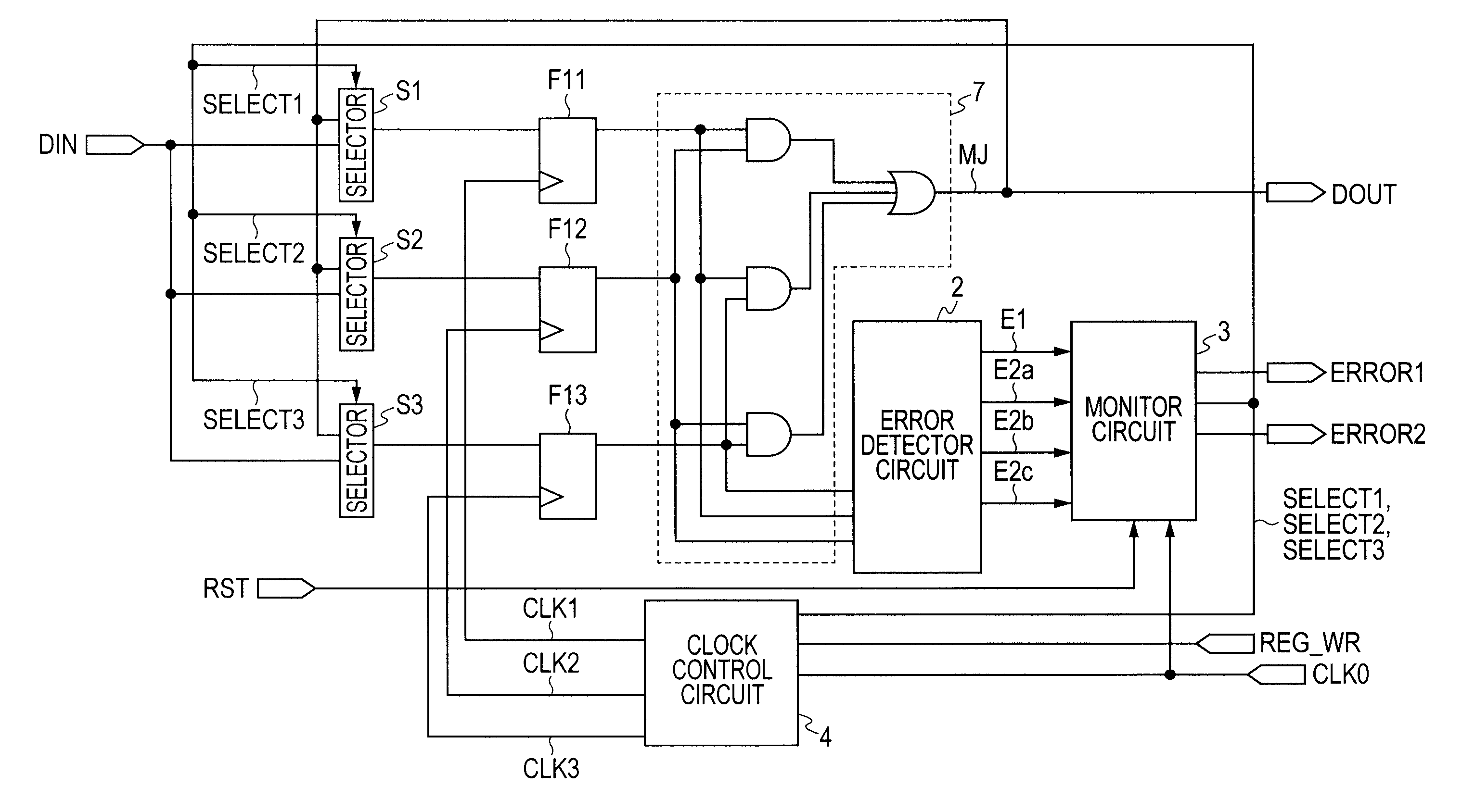
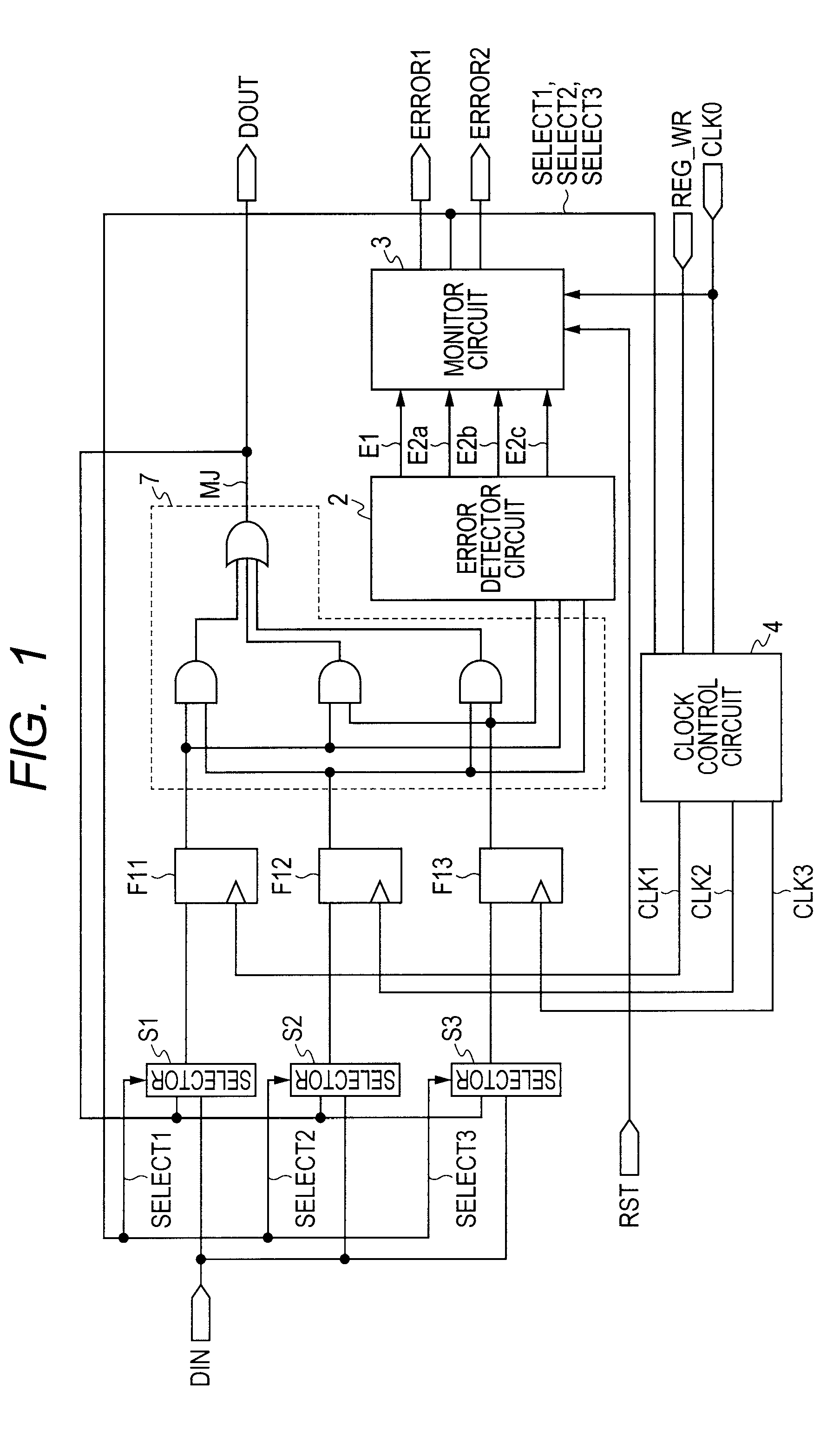
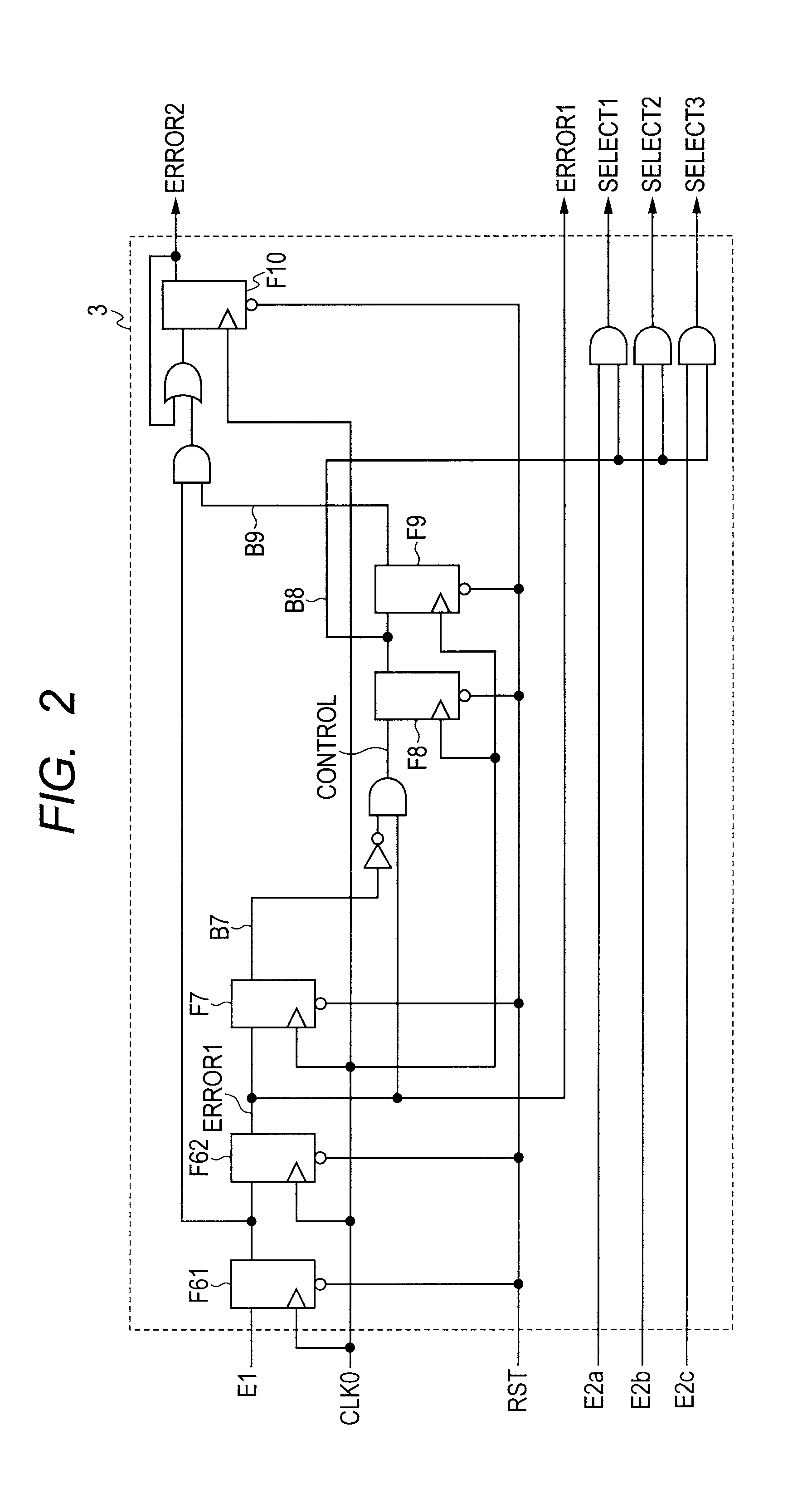
[0043]First, a configuration of a semiconductor integrated circuit pertaining to an embodiment disclosed herein is described, using FIGS. 1 thru 3. FIG. 1 is a block diagram showing an overall configuration of a semiconductor integrated circuit pertaining to a first embodiment. FIG. 2 is a circuit diagram showing an example of a monitor circuit that is used in the semiconductor integrated circuit pertaining to the first embodiment. FIG. 3 is a circuit diagram showing an example of a clock control circuit that is used in the semiconductor integrated circuit pertaining to the first embodiment.

[0044]The semiconductor integrated circuit pertaining to the first embodiment, as shown in FIG. 1, is equipped with three flip-flops F11, F12, F13, a majority circuit 7, an error detector circuit 2, a monitor circuit 3, a clock control circuit 4, and three selectors S1, S2, S3.

[0045]Respective input terminals of the flip-flops F11, F12, F13 (hereinafter may be referred to as a flip-flop F1 simply...

second embodiment

[0084]A configuration of a semiconductor integrated circuit pertaining to a second embodiment, using FIG. 7. FIG. 7 is a block diagram showing an overall configuration of a semiconductor integrated circuit pertaining to the second embodiment. While the first embodiment has been described with regard to a case where the monitor circuit 3 monitors the outputs from the flip-flops, which are input to one majority circuit 7, the semiconductor integrated circuit in the second embodiment is adapted to monitor the outputs from the flip-flops, which are input to a plurality of majority circuits, at the same time.

[0085]In FIG. 7, the monitor circuit 3 of the second embodiment is configured such that error signals from error detector circuits 2 in other peripheral circuits 5, 6 are additionally input to the monitor circuit 3 of the first embodiment. In particular, error signals E3, E4a, E4b, E4c from an error detector circuit 2, not shown, in a peripheral circuit 5 and error signals E5, E6a, E...


PUM


Abstract

A semiconductor integrated circuit pertaining to the present invention comprises a plurality of storage elements for storing and holding an input signal, a majority circuit that outputs a result of a majority decision of outputs from the plurality of storage elements; an error detector circuit that detects a mismatch among the outputs of the plurality of storage elements and outputs error signals; and a monitor circuit that monitors the error signals from the error detector circuit, wherein the monitor circuit, based on the error signals, orders a refresh action that rewrites data for rectification to a storage element in which an output mismatch occurs out of the plurality of storage elements and, if rewrite and rectification by the refresh action are unsuccessful, sends a notification to an external unit or process.

Description

CROSS-REFERENCE TO RELATED APPLICATIONS[0001]The disclosure of Japanese Patent Application No. 2010-50785 filed on Mar. 8, 2010 including the specification, drawings and abstract is incorporated herein by reference in its entirety.BACKGROUND[0002]1. Field of the Invention[0003]The present invention relates to a semiconductor integrated circuit and more particularly to a semiconductor integrated circuit equipped with a plurality of storage elements for storing and holding an input signal and a majority circuit that outputs a result of a majority decision of outputs from these storage elements.[0004]2. Description of Related Art[0005]Functional safety standard IEC 61508 (functional safety of electrical, electronic, and programmable electronic safety-related systems) was established in 2000. In Europe, it is obligated to obtain a functional safety certification on an ECU level with regard to a motor vehicle, inter alia, before obtaining a certification as the motor vehicle. This is for...

Claims


Application Information

Patent Timeline
Patent Type & Authority Applications(United States)
IPC IPC(8): H03M13/05G06F11/10
CPCG06F11/10G06F11/183G06F11/0793H03M13/05H03K19/007
Inventor NAKAMURA, KOICHI
Owner RENESAS ELECTRONICS CORP
Learn More