Tandem photovoltaic device with dual function semiconductor layer

a photovoltaic device and semiconductor layer technology, applied in the direction of pv power plants, non-metal conductors, conductors, etc., can solve the problems of increasing capital costs, reducing the efficiency of photogenerated charge carriers, and using separate interlayers, etc., to achieve high quality

Inactive Publication Date: 2011-09-15
UNITED SOLAR OVONIC
View PDF2 Cites 6 Cited by
  • Summary
  • Abstract
  • Description
  • Claims
  • Application Information

AI Technical Summary

Benefits of technology

[0009]Disclosed is a tandem photovoltaic device which is comprised of a first and a second photovoltaic triad. Each triad is comprised of a body of substantially intrinsic semiconductor material interposed between a body of p-doped semiconductor material and a body of n-doped semiconductor material. These triads are disposed in a stacked optical and electrical series relationship such that the first triad is closer to the light-incident surface of the photovoltaic device than is the second triad. According to the present invention, the body of n-doped semiconductor material of the first triad is comprised of a dual function, n-doped, hydrogenated, silicon-oxygen material. This dual function semiconductor material is further characterized in that in the operation of the photovoltaic device it establishes a high quality tunnel junction with the p-doped layer of the second triad. In the operation of the photovoltaic device, the dual function layer operates to create a field in the intrinsic body of the first triad which separates photogenerated charge carrier pairs formed therein by absorbed photons. The dual function layer also operates as a partially reflective layer which directs a portion of those photons striking it back into the intrinsic body of the first triad.

Problems solved by technology

The problem is that a thicker intrinsic layer is not as effective in collecting photogenerated charge carriers because of light induced degradation known as the “Staebler Wronski” degradation.
While there are a number of advantages attendant upon the incorporation of a light-reflective interlayer into a tandem photovoltaic device, the use of a separate interlayer also serves to complicate device manufacture and performance.
Further, capital costs increase because extra chambers are required for the vacuum deposition of the interlayer.
Additionally, the interlayer can add additional series resistance to the device thereby degrading its overall efficiency of the tandem photovoltaic devices.
The presence of a separate interlayer body can interfere with the formation of the tunnel junction.

Method used


Image

  • Tandem photovoltaic device with dual function semiconductor layer
  • Tandem photovoltaic device with dual function semiconductor layer
  • Tandem photovoltaic device with dual function semiconductor layer

Examples


Embodiment Construction

material may optionally include carbon in and amount of up to 10 atomic percent.

BRIEF DESCRIPTION OF THE DRAWINGS

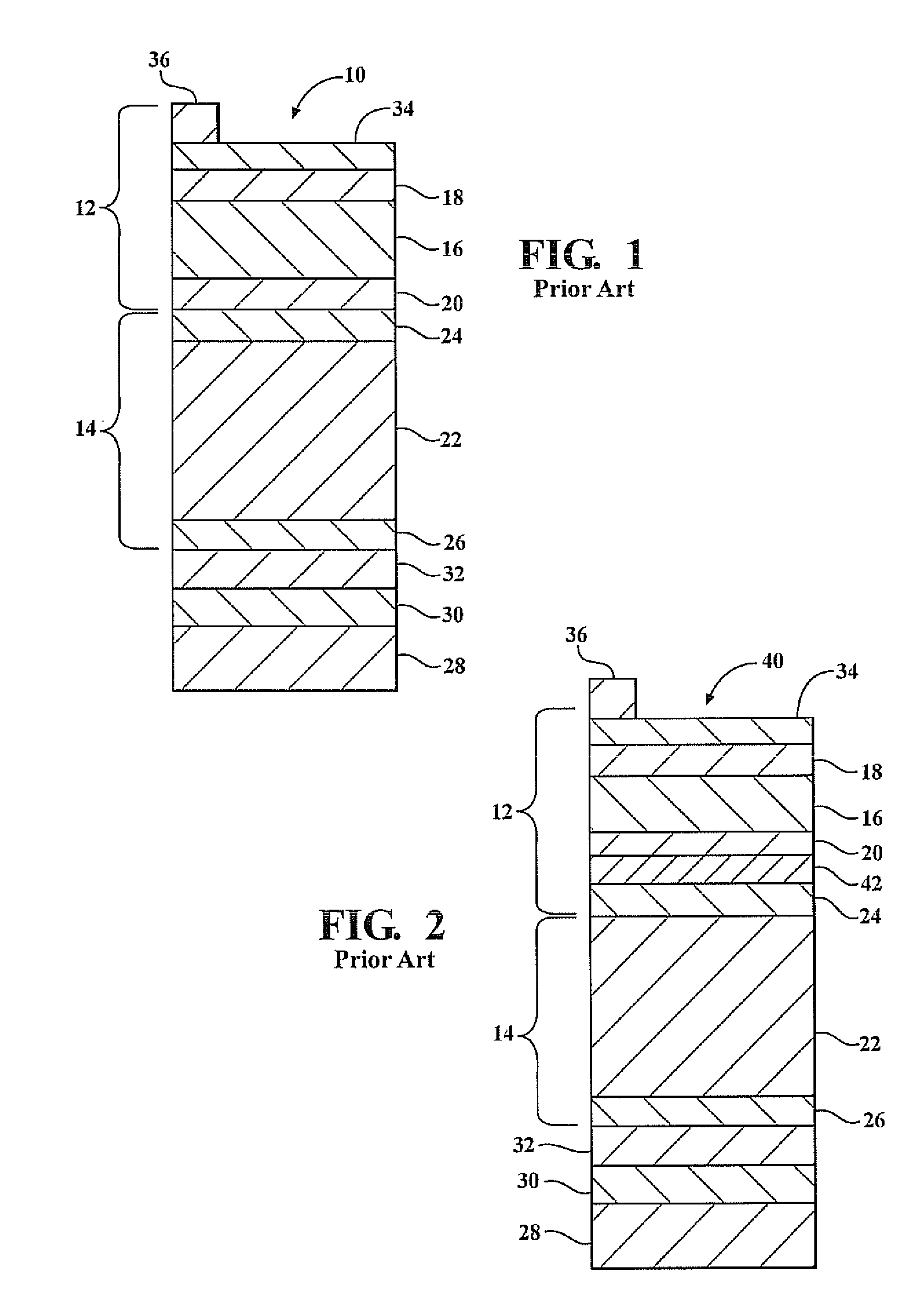
[0013]FIG. 1 is a cross-sectional view of a generalized tandem photovoltaic device of the prior art;

[0014]FIG. 2 is a cross-sectional view of a tandem photovoltaic device of the prior art including a discrete, reflective interlayer; and

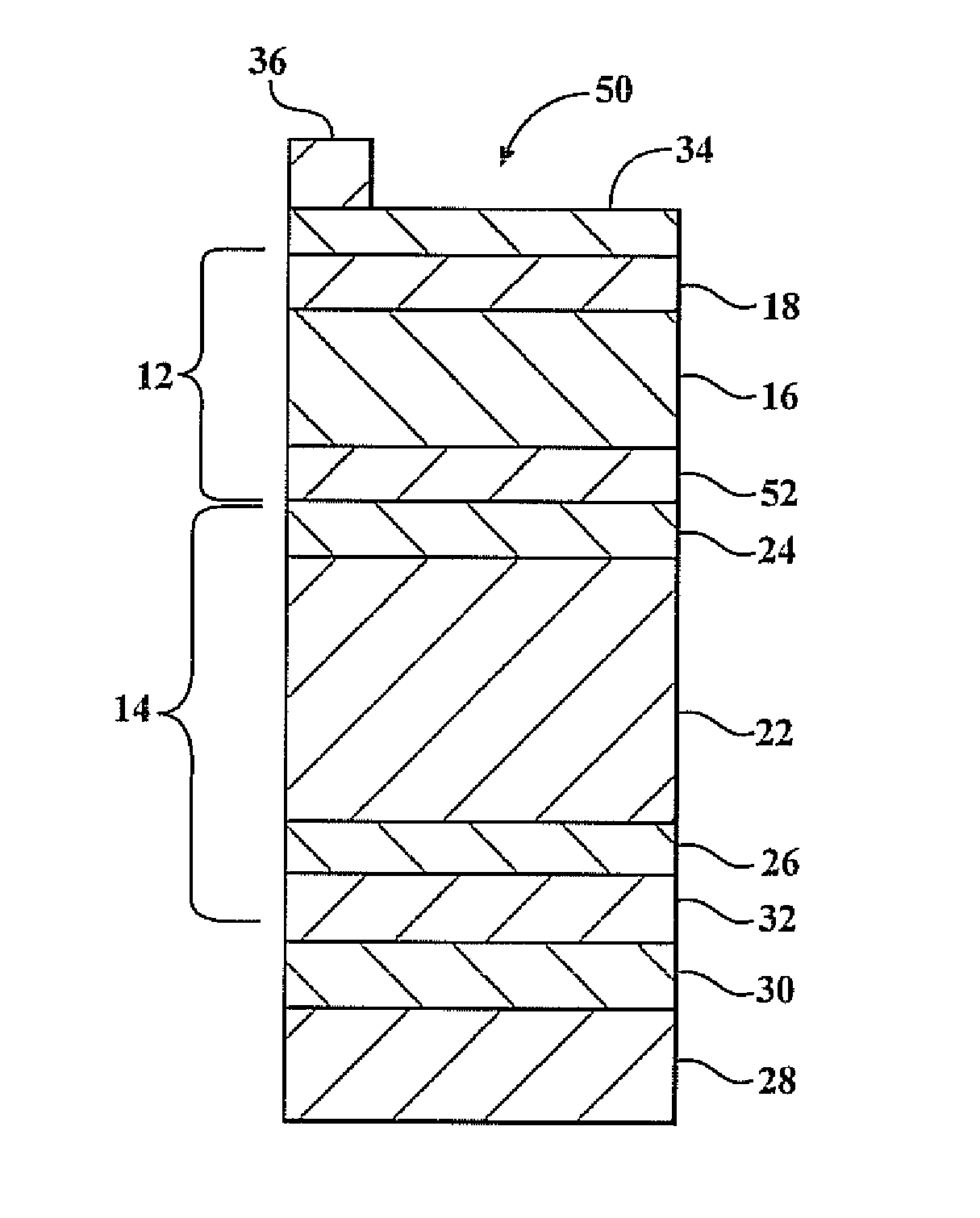
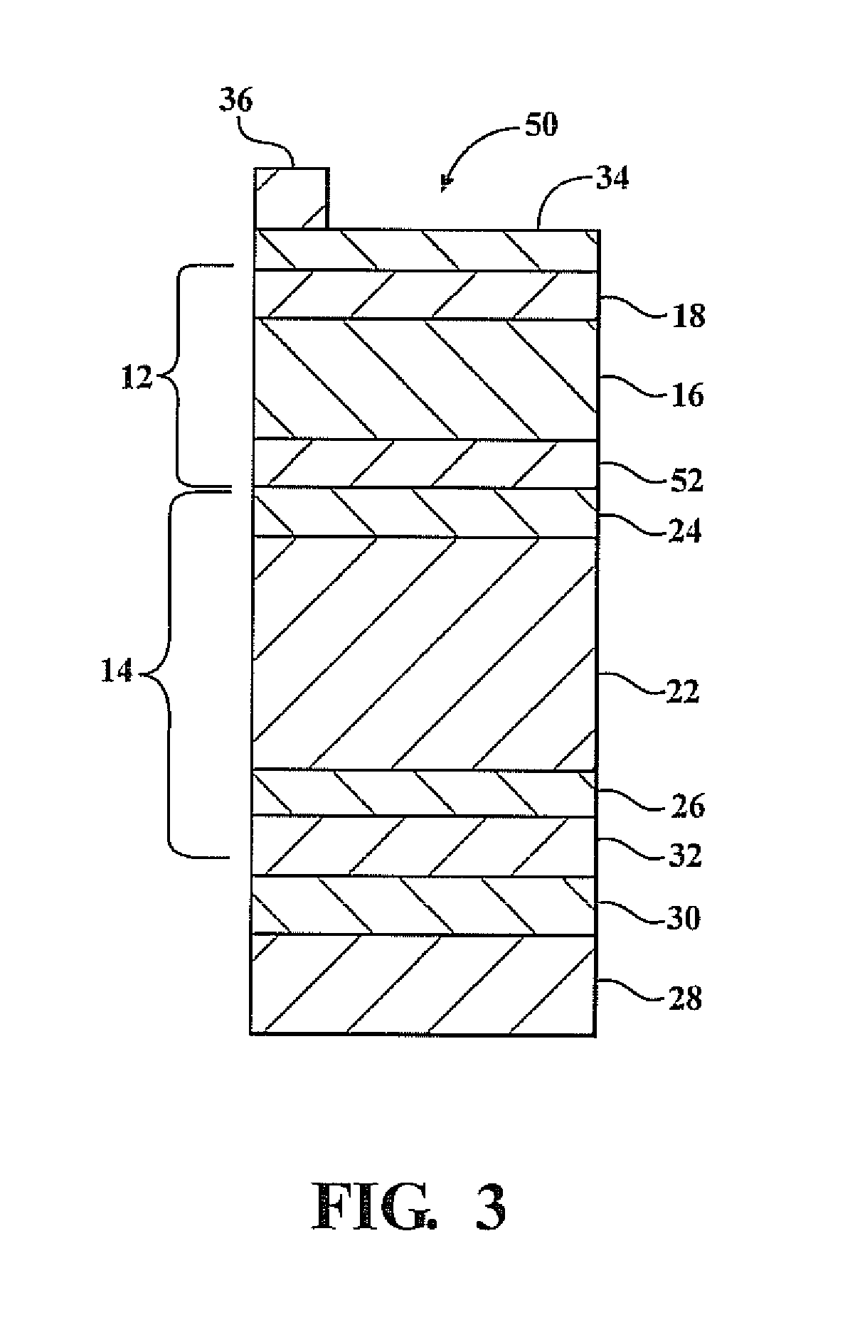
[0015]FIG. 3 is a cross-sectional view of a tandem photovoltaic device of the present invention incorporating a dual function layer.

DETAILED DESCRIPTION OF THE PREFERRED EMBODIMENTS

[0016]In accord with the present invention, tandem photovoltaic devices are fabricated to include a dual function layer of semiconductor material. This semiconductor layer operates as an active electronic element of the device, and in that regard participates in the generation and / or collection of photogenerated carrier pairs. The layer also functions to reflect light back through the other active layers of the photovoltaic device wherein it is absorbed to genera...


PUM

PropertyMeasurementUnit
short circuit currentaaaaaaaaaa
open circuit voltageaaaaaaaaaa
short circuit currentaaaaaaaaaa

Abstract

A tandem photovoltaic device includes at least two photovoltaic cells stacked in an optical and electrical series relationship. At least one of the tandem cells includes a dual function semiconductor layer fabricated from a dual function semiconductor material. This dual function layer is an electronically active constituent of the cell. The dual function layer also is optically active and creates a reflective condition which redirects a portion of the light which has passed through the cell back through the cell's active layers to photo generate additional photocurrent. Use of the dual function material eliminates the need for incorporating separate semiconductor and reflective layers in a photovoltaic device. Further disclosed are exemplary formulations of some dual function materials.

Description

STATEMENT OF GOVERNMENT INTEREST[0001]This invention was made with government support under contract DE-FC36-07GO17053 awarded by the Department of Energy. The United States Government has certain rights in the invention.FIELD OF THE INVENTION[0002]This invention relates generally to photovoltaic devices. More specifically the invention relates to tandem photovoltaic devices comprised of stacked photovoltaic cells. In particular the invention relates to tandem photovoltaic devices in which one of the electronically active semiconductor layers of at least one of the stacked cells is a dual function layer which also acts as a light-reflective layer.BACKGROUND OF THE INVENTION[0003]Tandem photovoltaic devices are constructed to include two or more photovoltaic cells stacked in an optical and electrical series relationship so that incident light passes, serially, through the stacked cells so as to generate a photo current. Since the cells are stacked in an electrical series relationship...

Claims


Application Information

Patent Timeline
Patent Type & Authority Applications(United States)
IPC IPC(8): H01L31/05H01B1/00H01B1/04
CPCH01L31/02168H01L31/0324H01L31/056Y02E10/52Y02E10/548H01L31/076
Inventor YAN, BAOJIEGUHA, SUBHENDUYANG, CHI
Owner UNITED SOLAR OVONIC
Why Eureka
Try Eureka