
Semiconductor device

a technology of semiconductor devices and breakdown voltages, applied in the direction of semiconductor devices, basic electric elements, electrical apparatus, etc., can solve the problem of reducing the space in the termination domain where the device structure is not formed, so as to achieve the effect of reducing the space in the termination domain and increasing the breakdown voltage of the semiconductor devi

Active Publication Date: 2011-09-15
DENSO CORP
View PDF4 Cites 23 Cited by
  • Summary
  • Abstract
  • Description
  • Claims
  • Application Information

AI Technical Summary

Benefits of technology

[0005]It is an object of the present teachings to provide a novel breakdown voltage structure which enables a space of a termination domain to be reduced compared to the conventional breakdown voltage structures, while increasing breakdown voltage.
[0008]In the above semiconductor device, the first conductive type floating region is not provided at the bottom of the gate trench while the first conductive type floating region is provided at the bottom of the termination trench. In other words, the first conductive type floating region is only formed in the termination domain. As a result, due to the floating region in the termination domain, a depletion layer extending from a P-N junction of the first drift region and the first body region when the semiconductor device is turned off spreads in a depth direction of the semiconductor substrate in the termination domain. Since the depletion layer spreads in the termination domain due to the floating region, the breakdown voltage of the semiconductor device can be increased. In addition, since the depletion layer spreads in the depth direction of the semiconductor substrate in the termination domain, the termination domain need not be laterally expanded. Therefore, the space of the termination domain can be reduced.

Problems solved by technology

As a result, there is a problem in that a space in the termination domain where a device structure is not formed must be enlarged.

Method used


Image

  • Semiconductor device
  • Semiconductor device
  • Semiconductor device

Examples


first embodiment

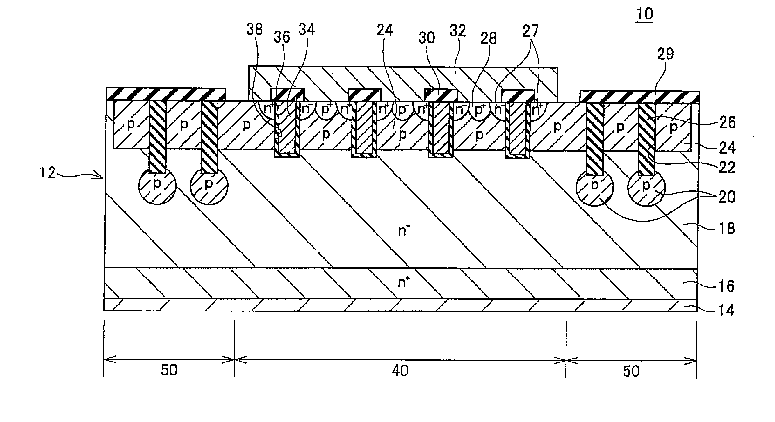
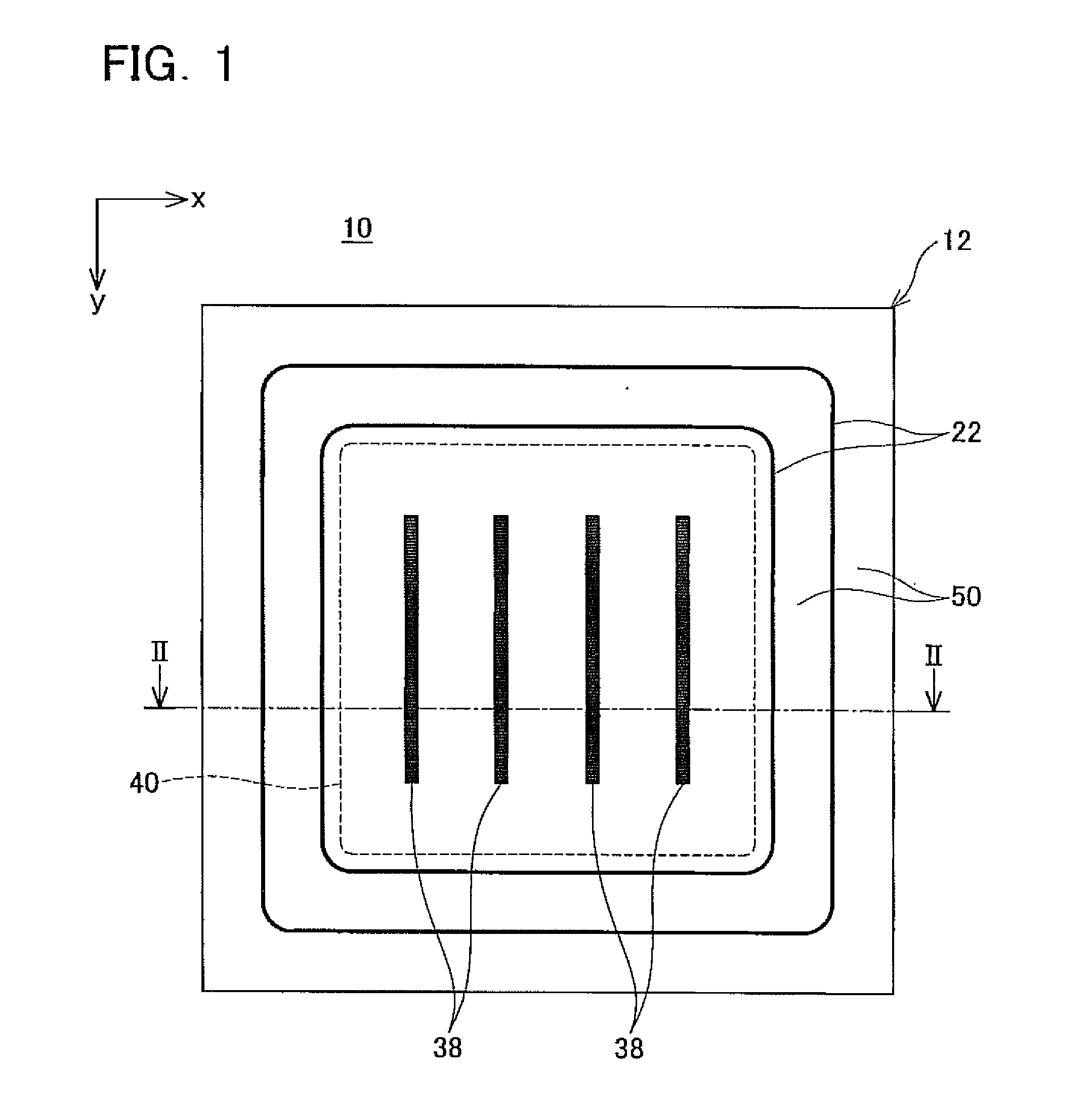
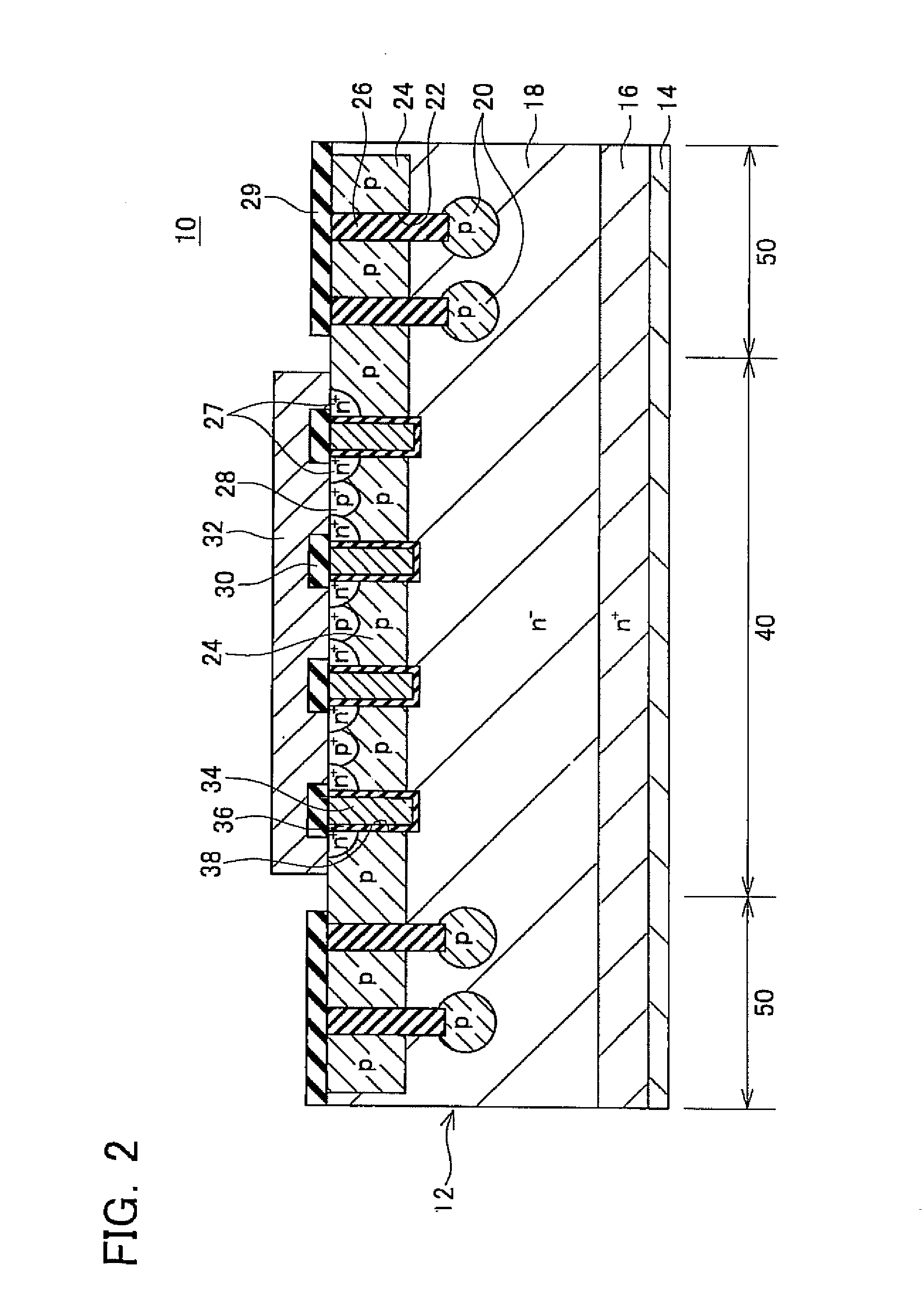
[0014]A semiconductor device 10 according to the first embodiment will now be described with reference to the drawings. As shown in FIG. 1, the semiconductor device 10 comprises an element domain 40 and a termination domain 50 that surrounds the element domain 40.

[0015]A plurality of gate trenches 38 is formed in the element domain 40. The gate trenches 38 extend in a y-direction in FIG. 1 and are arranged at regular intervals in an x-direction in FIG. 1. Termination trenches 22 are formed in the termination domain 50. Each of the termination trenches 22 surrounds the element domain 40. The element domain 40 and the termination domain 50 are formed on a same semiconductor substrate 12. A known substrate (e.g., a silicon substrate (Si substrate), a silicon carbide substrate (SiC substrate), and the like) can be used as the semiconductor substrate 12.

[0016]First, a configuration of the element domain 40 will be described. As shown in FIG. 2, a vertical field effect transistor (MOSFET)...

second embodiment

[0033]A semiconductor device 70 according to a second embodiment will now be described with reference to FIG. 4. The semiconductor device 70 according to the second embodiment differs from the semiconductor device 10 according to the first embodiment in that a body region 72 is formed so as to extend laterally to a side surface of a semiconductor substrate 78 and that a termination trench 74 is further provided. Other components of the semiconductor device 70 according to the second embodiment are similar to those of the first embodiment. Therefore, similar portions to the semiconductor device 10 according to the first embodiment will be denoted by same reference numerals and a description thereof will be omitted.

[0034]In the semiconductor substrate 78 used in the semiconductor device 70 according to the second embodiment, the body region 72 is laminated over an entire upper surface of a drift region 71. Therefore, the body region 72 is exposed at the side surface of the semiconduct...


PUM


Abstract

A semiconductor device 10 may comprise an element domain 40 and a termination domain 50 that surrounds the element domain 40. The element domain 40 and the termination domain 50 respectively may comprise a second conductive type drift region 18. A gate trench 38 may be provided in the element domain 40. The termination domain 50 may be provided with a termination trench 22 surrounding the element domain. A first conductive type floating region surrounded by the drift region 18 is not provided at a bottom of the gate trench 38, and a first conductive type floating region 20 surrounded by the drift region 18 is provided at a bottom of the termination trench 22.

Description

CROSS-REFERENCE TO RELATED APPLICATION[0001]This application claims priority to Japanese Patent Application No. 2010-51794 filed on Mar. 9, 2010, the contents of which are hereby incorporated by reference into the present application.TECHNICAL FIELD[0002]The present application relates to a technique for increasing breakdown voltage of a semiconductor device.DESCRIPTION OF RELATED ART[0003]A semiconductor device provided with an element domain and a termination domain that surrounds the element domain is known. In a semiconductor device of this type, typically, a device structure (e.g., a MOS (Metal Oxide Semiconductor) or an IGBT (Insulated Gate Bipolar Transistor)) is formed in the element domain and a structure for increasing breakdown voltage (hereinafter referred to as a “breakdown voltage structure”) is formed in the termination domain. For example, an FLR (Field Limiting Ring) structure is well known as the breakdown voltage structure. The FLR structure enables a depletion la...

Claims


Application Information

Patent Timeline
Patent Type & Authority Applications(United States)
IPC IPC(8): H01L29/78
CPCH01L29/0623H01L29/0653H01L29/7813H01L29/1095H01L29/7811H01L29/0661
Inventor TAKAYA, HIDEFUMI
Owner DENSO CORP
Features
  • Generate Ideas
  • Intellectual Property
  • Life Sciences
  • Materials
  • Tech Scout
  • Unparalleled Data Quality
  • Higher Quality Content
  • 60% Fewer Hallucinations
Learn More