Method for phase transition of amorphous material

Inactive Publication Date: 2011-09-15
UNIV IND COOP GRP OF KYUNG HEE UNIV
View PDF3 Cites 2 Cited by
  • Summary
  • Abstract
  • Description
  • Claims
  • Application Information

AI Technical Summary

Benefits of technology

[0017]According to exemplary embodiments of the invention, the method can crystallize an amorphous material for use in fabrication of a thin film transisto

Problems solved by technology

However, the laser heat treatment is not suitable for fabrication of polycrystalline silicon on a large area substrate due to problems such as non-uniform phase transition, use of expensive systems, and low yields.
In this method, however, crystallization requires a long period of time causing low productivity and is performed at high temperature making it difficu

Method used


Image

  • Method for phase transition of amorphous material
  • Method for phase transition of amorphous material
  • Method for phase transition of amorphous material

Examples


Example

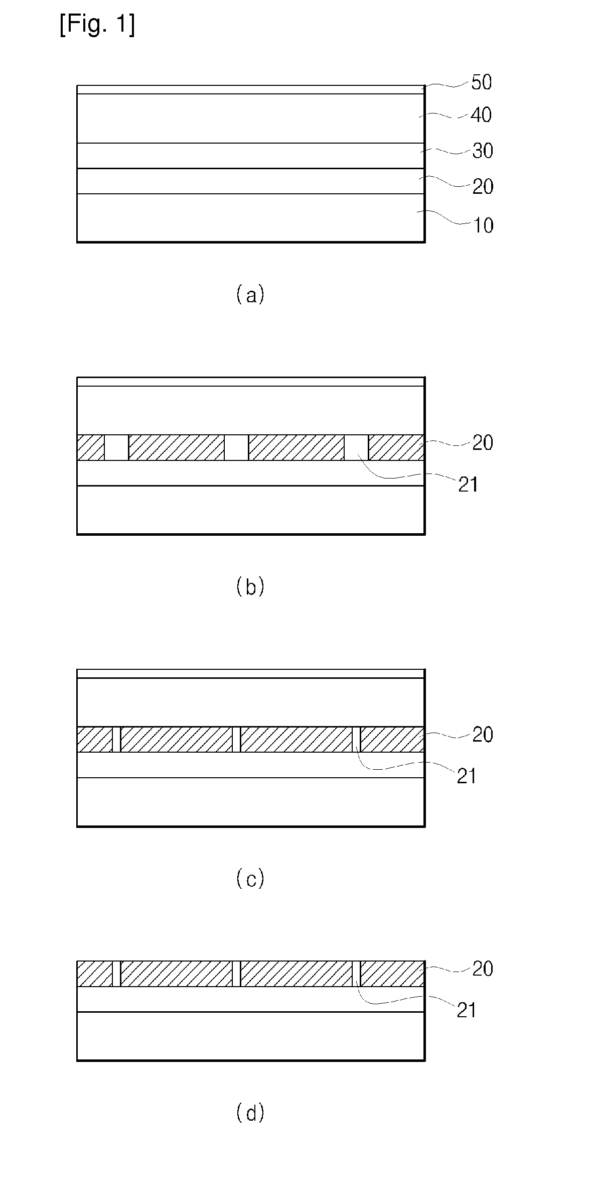
[0024]According to an embodiment of the present invention, a method for phase transition of an amorphous material based on metal induced lateral crystallization includes forming an amorphous silicon layer on a substrate, depositing a Ni metal layer on part of the amorphous silicon layer, and heat-treating the amorphous silicon layer to cause phase transition of the amorphous silicon, wherein the Ni metal layer is deposited to an average thickness of 0.79 Å or less.

[0025]Mode for the Invention

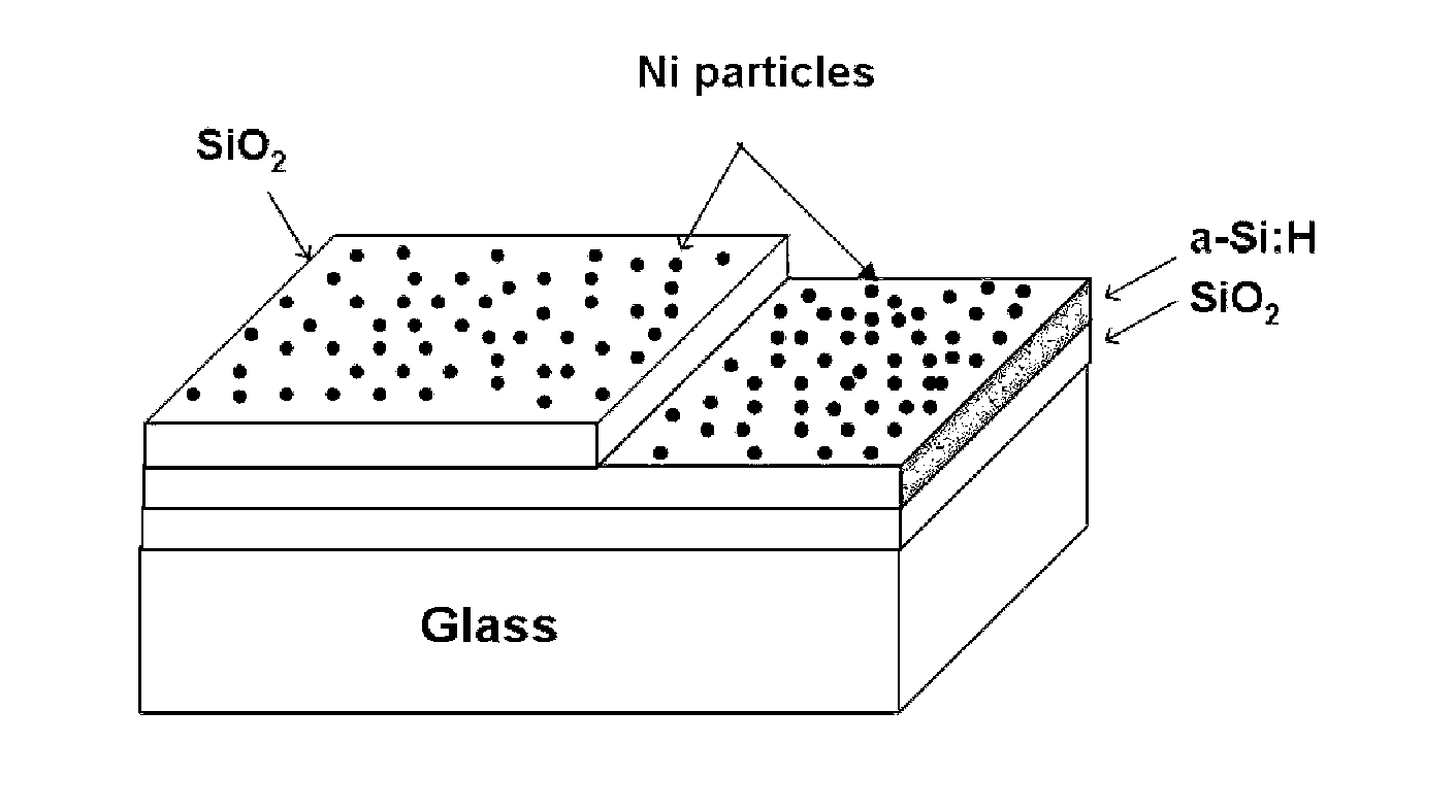
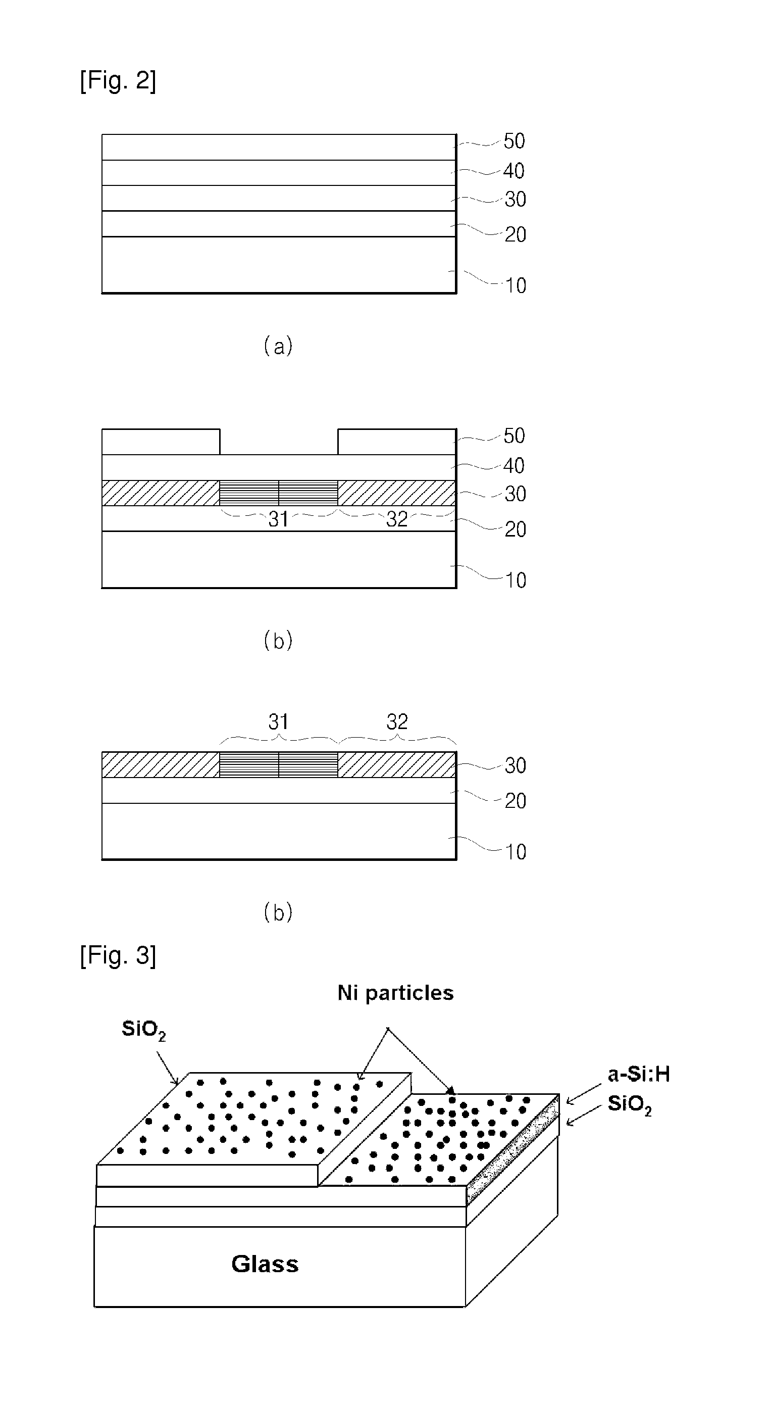
[0026]FIG. 1 is a flow diagram illustrating crystallization of amorphous silicon based on Ni-MILC.

[0027]In a method for phase transition of an amorphous material for use in fabrication of a thin film transistor according to an embodiment of the invention, the thickness of a metal deposited on a substrate is adjusted during metal induced lateral crystallization used for crystallization of the amorphous material, thereby minimizing current leakage.

[0028]Next, the metal induced lateral crystallizat...


PUM


Abstract

Disclosed herein is a method of crystallizing an amorphous material for use in fabrication of thin film transistors. The method includes forming an amorphous silicon layer on a substrate, depositing a Ni metal layer on part of the amorphous silicon layer, and heat-treating the amorphous silicon layer to cause phase transition of the amorphous silicon, wherein the Ni metal layer is deposited to an average thickness of 0.79 Å or less. The method can crystallize an amorphous material for use in thin film transistors using the metal induced lateral crystallization while restricting thickness and density of Ni, thereby minimizing current leakage in the thin film transistor.

Description

TECHNICAL FIELD[0001]The present invention relates to a method of crystallizing an amorphous material for use in fabrication of thin film transistors and, more particularly, to a metal induced lateral crystallization (MILC) method.BACKGROUND ART[0002]Thin film transistors (TFTs) refer to a switching element that employs a poly-crystalline silicon thin film as an active layer, and are generally used for active elements of active matrix liquid crystal displays and switching elements and peripheral circuits of electric light emitting devices.[0003]In general, the thin film transistor is fabricated by direct deposition, high temperature heat treatment or laser heat treatment. Particularly, the laser heat treatment is preferred to the other processes due to merits such as crystallization (also referred to as phase transition) at low temperatures of 400° C. or less and high field effect mobility. However, the laser heat treatment is not suitable for fabrication of polycrystalline silicon ...

Claims


Application Information

Patent Timeline
IPC IPC(8): H01L21/20
CPCH01L21/02532H01L27/1277H01L21/02672H10B99/00
Inventor JANG, JINOH, JAE-HWANKANG, DONG-HANCHEON, JUN-HYUK
Owner UNIV IND COOP GRP OF KYUNG HEE UNIV
Why Eureka
Try Eureka