
Doping of semiconductor substrate through carbonless phosphorous-containing layer

Active Publication Date: 2011-09-15
GLOBALFOUNDRIES US INC
View PDF2 Cites 0 Cited by
  • Summary
  • Abstract
  • Description
  • Claims
  • Application Information

AI Technical Summary

Problems solved by technology

If the dopant concentration is too low, or if the source and drain are too distant, the threshold voltage will be undesirably high.
If the dopant concentration is too high, or if the source and drain regions are too close, the threshold voltage will be undesirably low, and the resistance in the unpowered state may be insufficient to prevent electron flow.
With prior art techniques, it is extremely difficult to achieve uniform doping across a large substrate due to dose variation.
In addition, it is difficult to control the doping profile.
In this approach, although the extent of doping can be controlled, the presence of carbonaceous materials in the silicon results in diffusion of carbon in the silicon and formation of unwanted carbides.

Method used


Image

  • Doping of semiconductor substrate through carbonless phosphorous-containing layer
  • Doping of semiconductor substrate through carbonless phosphorous-containing layer
  • Doping of semiconductor substrate through carbonless phosphorous-containing layer

Examples


Embodiment Construction

[0020]Detailed embodiments of the present invention are disclosed herein; however, it is to be understood that the disclosed embodiments are merely illustrative of the invention that may be embodied in various forms. In addition, each of the examples given in connection with the various embodiments of the invention is intended to be illustrative, and not restrictive. Further, the figures are not necessarily to scale, some features may be exaggerated to show details of particular components. Therefore, specific structural and functional details disclosed herein are not to be interpreted as limiting, but merely as a representative basis for teaching one skilled in the art to variously employ the present invention.

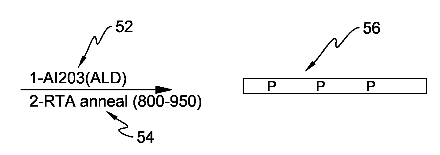
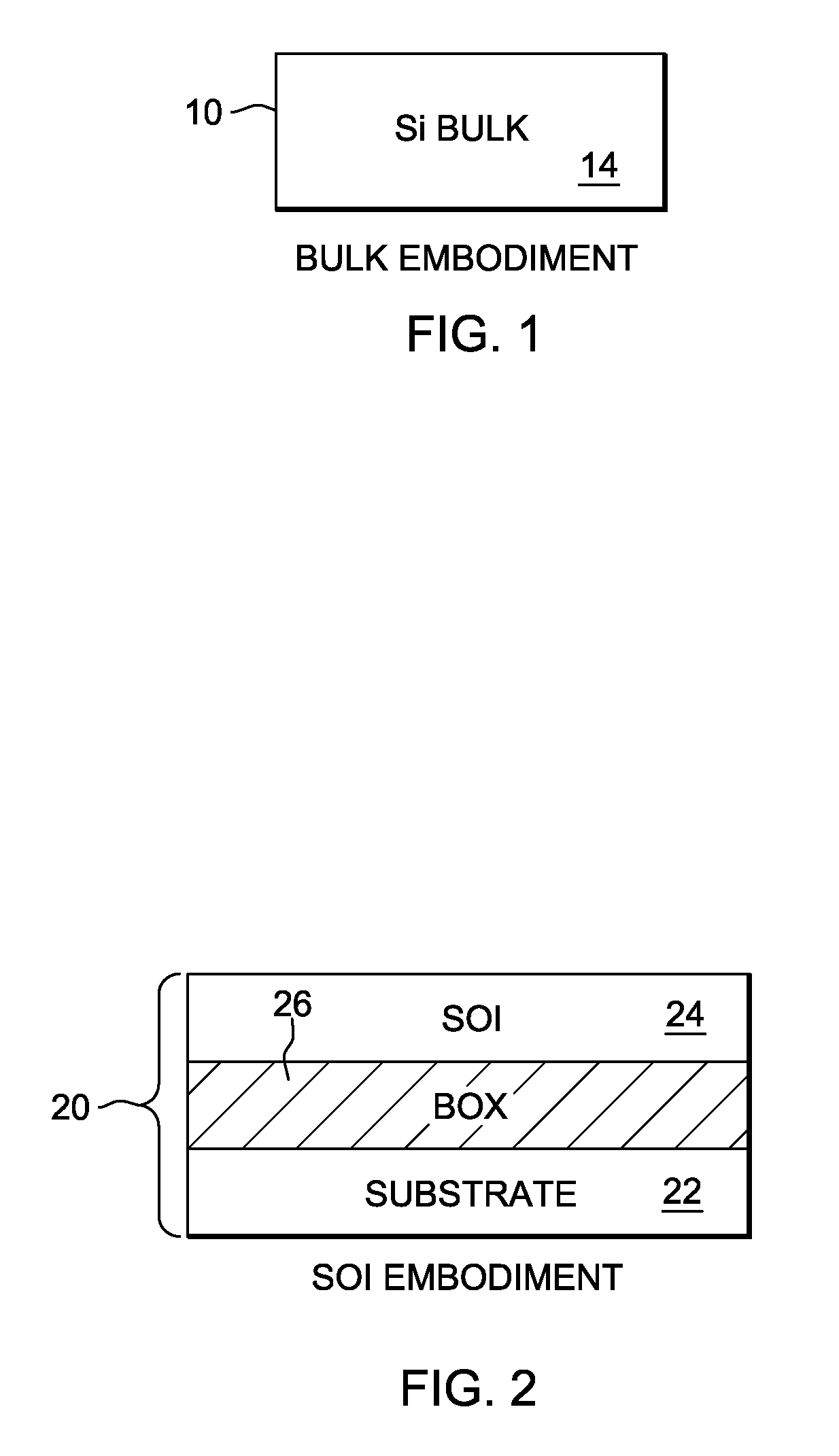
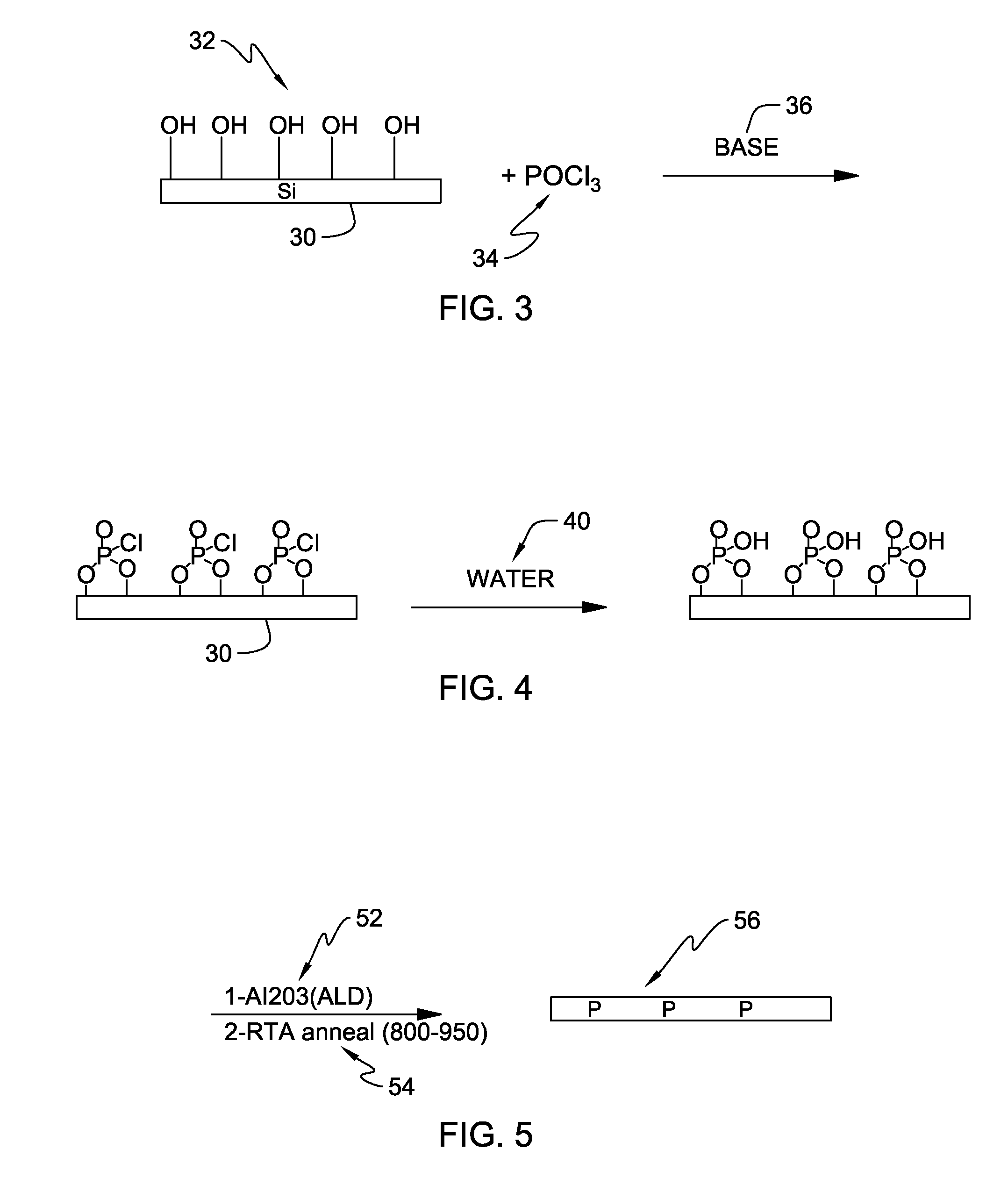
[0021]FIGS. 1 and 2 show devices 10 and 20 that may be used in the present invention. Device 10 includes a bulk semiconductor material 14. Device 20 is a semiconductor-on-insulator material including semiconductor layers 22 and 24 and insulating layer 26.

[0022]With reference ...


PUM


Abstract

A method and system are disclosed for doping a semiconductor substrate. In one embodiment, the method comprises forming a carbon free layer of phosphoric acid on a semiconductor substrate, and diffusing phosphorous from the layer of phosphoric acid in the substrate to form an activated phosphorous dopant therein. In an embodiment, the semiconductor substrate is immersed in a solution of a phosphorous compound to form a layer of the phosphorous compound on the substrate, and this layer of phosphorous is processed to form the layer of phosphoric acid. In an embodiment, this processing may include hydrolyzing the layer of the phosphorous compound to form the layer of phosphoric acid. In one embodiment, an oxide cap layer is formed on the phosphoric acid layer to form a capped substrate. The capped substrate may be annealed to diffuse the phosphorous in the substrate and to form the activated dopant.

Description

BACKGROUND OF THE INVENTION[0001]1. Field of the Invention[0002]This invention, generally, relates to semiconductor fabrication, and more specifically, to doping of semiconductor materials.[0003]2. Background Art[0004]Semiconductor devices are used in a wide variety of applications including diodes, photodetectors, photocells, transistors, and integrated circuits. Silicon and germanium are commonly used in such electronic devices. In particular, silicon is the most widely used material in semiconductor devices due to its low cost, relatively simple processing, and useful temperature range. Further, the electronic properties and behavior of silicon and germanium can be relatively easily controlled by the addition of doping elements, for example, in the manufacture of P-I-N and N-I-P diodes.[0005]In a conventional practice, semiconductor fabrication begins with the provision of a semiconductor wafer, comprising silicon formed in a regular, crystalline structure. A circuit pattern is d...

Claims


Application Information

Patent Timeline
IPC IPC(8): H01L21/225B05C3/02
CPCH01L21/225H01L21/2254
Inventor AFZALI-ARDAKANI, ALIFARMER, DAMON B.SEKARIC, LIDIJA
Owner GLOBALFOUNDRIES US INC
Learn More