Solar battery unit

Inactive Publication Date: 2011-09-22
NAT TAIWAN UNIV
View PDF1 Cites 9 Cited by
  • Summary
  • Abstract
  • Description
  • Claims
  • Application Information

AI Technical Summary

Benefits of technology

[0044]Hence, the present invention teaching forming a nano rough layer on electrodes randomly and by a variable means, or forming a nano rough structure randomly distributed across the substrate by a processing process performed by a variable means, so as to maximize utilization of residual solar energy left behind after absorption of solar energy by the semiconductor active layer and feed back the energy to the semiconductor active layer with a view to optimizing the recycling of solar energy and absorption of

Problems solved by technology

Given a drift distance of greater than 100 nanometers, recombination of electrons and holes occurs readily to thereby cause a waste of absorbed solar energy.
Although it is necessary for a solar energy device to be thin, but the solar energy device may be too thin to take in solar energy thoroughly.
However, the prior art of forming the aforesaid holes is limited by difficulty in c

Method used


Image

  • Solar battery unit
  • Solar battery unit
  • Solar battery unit

Examples


Example

First Embodiment

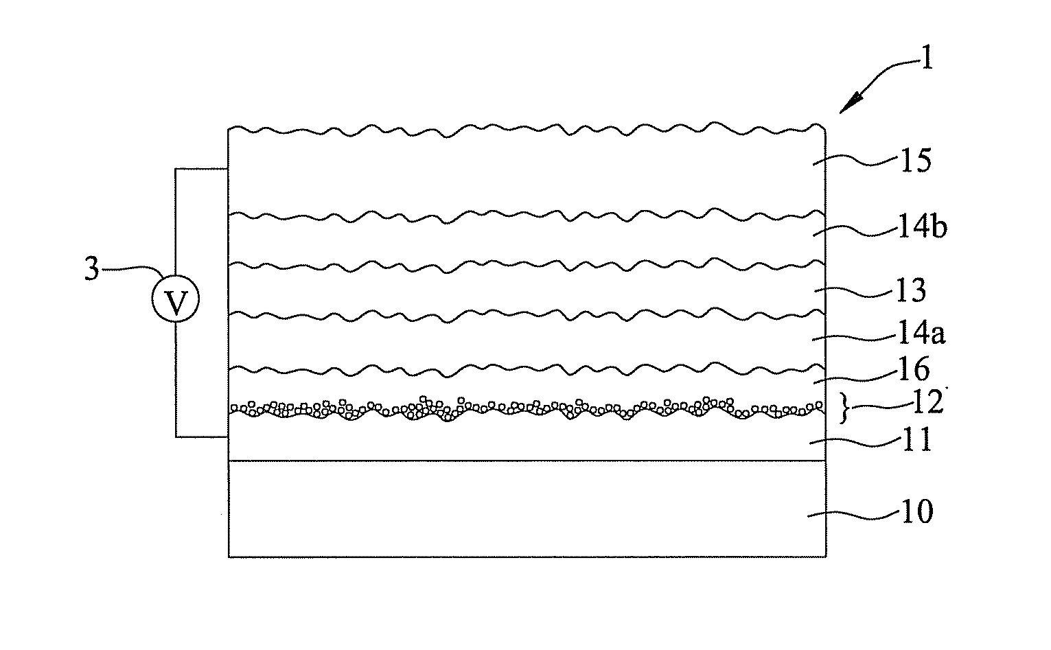
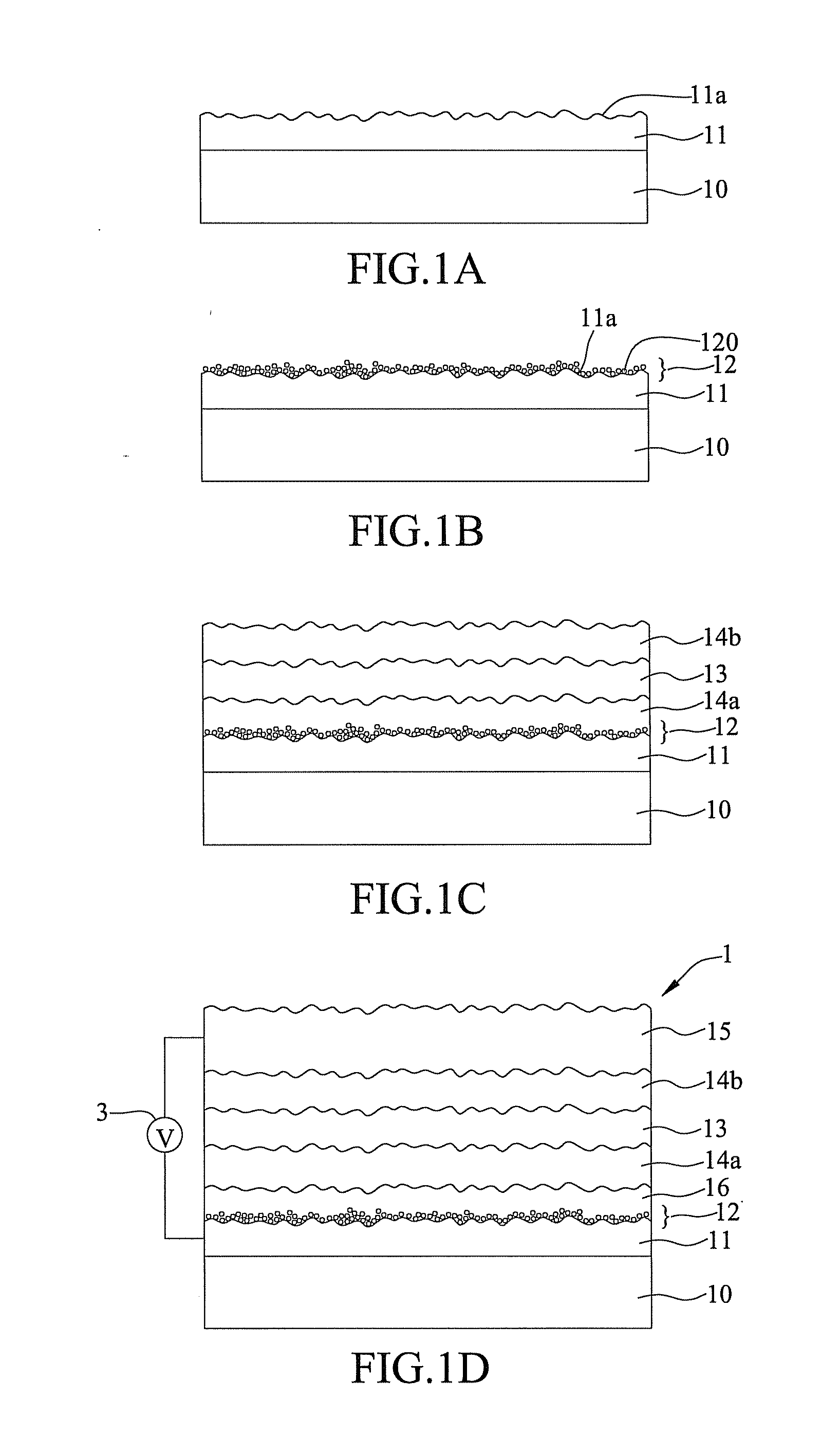
[0054]Referring to FIGS. 1A through 1D, there are shown schematic cross-sectional views of a method for fabricating a solar battery unit 1 in a first embodiment according to the present invention.

[0055]Referring to FIG. 1A, a first electrode 11 is provided, and the first electrode 11 is disposed on a substrate 10. The material of which the substrate 10 is made is a transparent material, paper, glass, a polymeric material, or a metallic material.

[0056]In this embodiment, the first electrode 11 is formed by applying a metallic material to the substrate 10, using sputtering, evaporation, spin coating, immersion, spraying, drying after dripping, organic metal chemical vapor deposition (MOCVD), electroplating, or a chemical reaction. The metallic material is Al, Au, Cu, Ag, Cr, Pt, Co, Ni, or Ti. In this embodiment, the material of which the first electrode 11 is made can also be a non-metallic material.

[0057]In this embodiment, the first electrode 11 has a convoluted sur...

Example

Second Embodiment

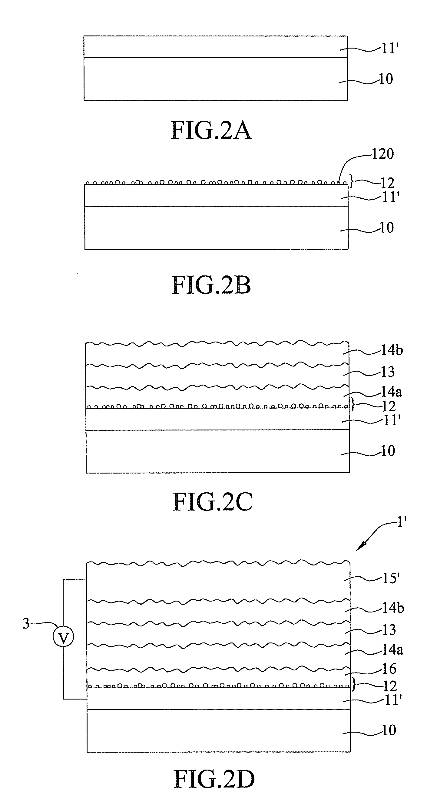
[0066]Referring to FIGS. 2A through 2D, there are shown schematic cross-sectional views of the method for fabricating a solar battery unit 1′ in a second embodiment according to the present invention. The difference between the second embodiment and the first embodiment is that, in the second embodiment, the first electrode 11′ and the second electrode 15′ are made of different material.

[0067]Referring to FIG. 2A, the first electrode 11′ is provided, and the first electrode 11′ is disposed on the substrate 10. In this embodiment, the material of which the first electrode 11′ is made is a transparent material, and thus the substrate 10 is also made of a transparent material. The first electrode 11′ has a flat surface.

[0068]Referring to FIG. 2B, the nano rough layer 12 is formed on the first electrode 11′, and the nano rough layer 12 comprises a plurality of metallic nanoparticles 120 stacked up. The plurality of metallic nanoparticles 120 is stacked up by spin coatin...

Example

Third Embodiment

[0073]Referring to FIGS. 3A through 3D, there are shown schematic cross-sectional views of the method for fabricating a solar battery unit 1″ in a third embodiment according to the present invention. The difference between the third embodiment and the second embodiment is that, in the third embodiment, a nano rough layer 12′ takes on a new structure.

[0074]Referring to FIG. 3A, the first electrode 11′ is provided, and the first electrode 11′ is disposed on the substrate 10. The material of which the first electrode 11′ and the substrate 10 are made is a transparent material.

[0075]Referring to FIG. 3B, the nano rough layer 12′ is formed on the first electrode 11′, and the nano rough layer 12′ comprises a metal membrane 121 and a plurality of metallic nanoparticles 120′ disposed on the first electrode 11′ and covered with the metal membrane 121.

[0076]There is no limitation on the material of which the metallic nanoparticles 120′ are made, though the material is preferab...


PUM


Abstract

A solar battery unit is proposed, including: a first electrode; a nano rough layer formed on the first electrode; a semiconductor active layer formed on the nano rough layer; and a second electrode formed on the semiconductor active layer, thereby enabling the nano rough layer formed on the first electrode to fully absorb solar energy not completely absorbed by the semiconductor active layer so as to allow solar energy to be fed back to the semiconductor active layer with a view to maximizing absorption of solar energy.

Description

BACKGROUND OF THE INVENTION[0001]1. Field of the Invention[0002]The present invention relates to solar energy elements, and more particularly, to a solar battery unit.[0003]2. Description of the Prior Art[0004]At present, organic semiconductor materials, of which solar energy devices are fabricated, are flexible, lightweight, thin, cheap to manufacture, and environmentally friendly. Organic semiconductors have lower carrier (electrons and holes) mobility rate than inorganic semiconductors and thus their electrons and holes have an extremely short drift distance, that is, less than 100 nanometers. Given a drift distance of greater than 100 nanometers, recombination of electrons and holes occurs readily to thereby cause a waste of absorbed solar energy. Although it is necessary for a solar energy device to be thin, but the solar energy device may be too thin to take in solar energy thoroughly.[0005]According to the prior art, to prevent recombination of electrons and holes, it is nece...

Claims


Application Information

Patent Timeline
IPC IPC(8): H01L31/0216H01L31/0224H01L31/0236
CPCH01L31/02168H01L31/022425Y02E10/50H01L31/0236H01L31/022466H01L31/02366
Inventor LEE, KANG-CHUANGLEE, CHIH-KUNGWU, WEN-JONGYANG, MIN-HUAKUO, PIN-HAN
Owner NAT TAIWAN UNIV
Why Eureka
Try Eureka