Semiconductor light emitting device and a production method thereof

Inactive Publication Date: 2011-09-22
STANLEY ELECTRIC CO LTD
View PDF13 Cites 1 Cited by
  • Summary
  • Abstract
  • Description
  • Claims
  • Application Information

AI Technical Summary

Benefits of technology

[0021]According to the invention, it is possible to provide a semiconductor light emi

Problems solved by technology

There are two disadvantages, however, in carrying out wet etching to form anisotropic irregularities on the semiconductor layer.
Second, such anisotropic irregularities tend to be formed in t

Method used


Image

  • Semiconductor light emitting device and a production method thereof
  • Semiconductor light emitting device and a production method thereof
  • Semiconductor light emitting device and a production method thereof

Examples


Embodiment Construction

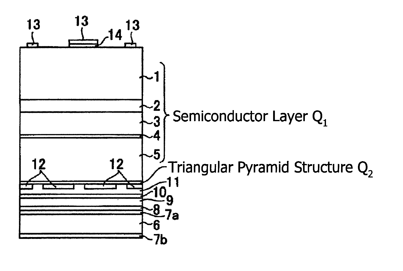
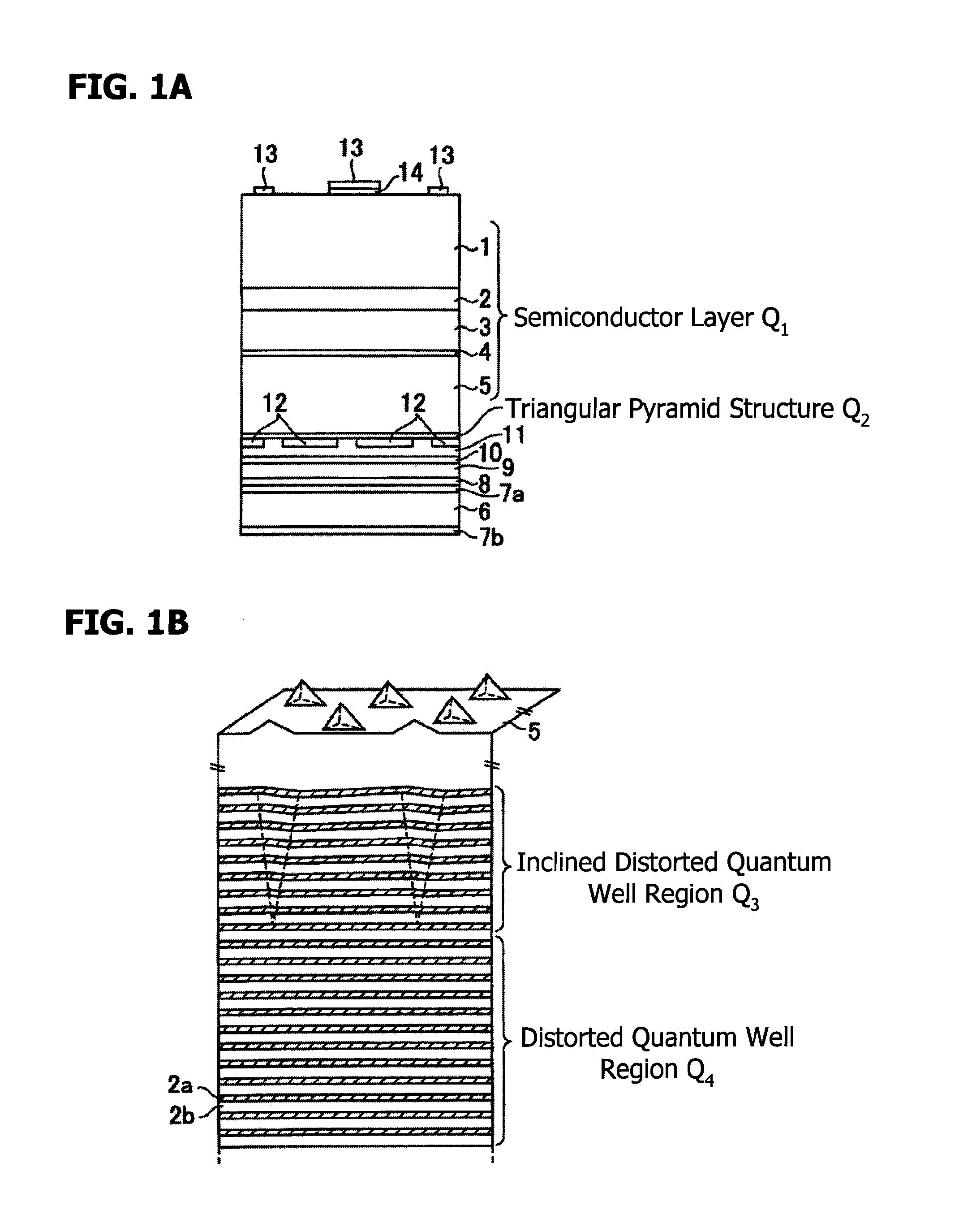
[0028]FIGS. 1A and 1B show a schematic diagram of a semiconductor light emitting device according to the embodiment.

[0029]See FIG. 1A. The semiconductor light emitting device according to the embodiment comprises an electrically conductive support substrate 6, ohmic metal layers 7a and 7b provided on either side of the electrically conductive support substrate 6, a contact layer 8, a composite joining layer 9, a barrier layer 10, and a reflecting electrode layer 11, the latter four being formed on the ohmic metal layer 7a. An insulation layer 12 is formed in some portions of the reflecting electrode layer 11.

[0030]A semiconductor layer of an AlGaInP based material is provided over the reflecting electrode layer 11 and the insulation layer 12. The semiconductor layer Q1 is a generally flat laminate that consists of a p-type transparent electrically conductive layer 5, a p-type AlGaInP interlayer 4, a p-type AlGaInP cladding layer 3, an AlGaInP active layer 2, and an n-type AlGaInP cl...


PUM


Abstract

A semiconductor light emitting device comprising a semiconductor layer of (AlyGa1-y)xIn1-xP (0<x≦1, 0≦y≦1) that consists of a first semiconductor layer of a first electrical conduction type, an active layer of a multiple quantum well structure containing a barrier layer and a distortion-containing well layer, a second semiconductor layer of a second electrical conduction type, and a third semiconductor layer of the second electrical conduction type, constructed in this order in the form of a generally flat laminate; a first electrode electrically connected to the first semiconductor layer; and a second electrode electrically connected to the third semiconductor layer; wherein part of the active layer facing the second semiconductor layer side is inclined from the surface of the active layer toward its normal, and the third semiconductor layer has a composition of Ga1-zInzP (0≦z≦0.35).

Description

CROSS-REFERENCE TO RELATED APPLICATION[0001]This application is based upon and claims the benefit of priority of the prior Japanese Patent Application No. JP 2010-064775, filed on Mar. 19, 2010, the entire contents of which are incorporated herein by reference.BACKGROUND OF THE INVENTION[0002]A) Field of the Invention[0003]The present invention relates to a semiconductor light emitting device and a production method thereof.[0004]B) Description of the Related Art[0005]Semiconductor light emitting devices comprising AlGaInP type semiconductor material are the most widely used of the light emitting devices including red and other light emitting diodes. These devices are commonly constructed as described below (see, for instance, Japanese Unexamined Patent Publication (Kokai) No. 2004-304090 as Patent document 1, which is incorporated herein by reference, and U.S. Pat. No. 5,008,718 as Patent document 2, which is incorporated herein by reference).[0006]A GaAs substrate is commonly used...

Claims


Application Information

Patent Timeline
IPC IPC(8): H01L33/06
CPCH01L33/0079H01L33/06H01L33/405H01L33/20H01L33/30H01L33/18H01L33/0093
Inventor TAMURA, WATARU
Owner STANLEY ELECTRIC CO LTD
Why Eureka
Try Eureka