Vertical integrated silicon nanowire field effect transistors and methods of fabrication

a technology of vertical integrated silicon nanowires and field effect transistors, which is applied in the direction of nanotechnology, electrical equipment, semiconductor devices, etc., can solve the problems of affecting the full potential of nanowire-based electronics, and affecting the realization of nanowire-based electronics

Inactive Publication Date: 2011-09-29
RGT UNIV OF CALIFORNIA
View PDF6 Cites 175 Cited by
  • Summary
  • Abstract
  • Description
  • Claims
  • Application Information

AI Technical Summary

Problems solved by technology

As semiconductor devices are scaled into the sub 50 nm regime, short-channel effects and poor sub-threshold characteristics begin to be problematic for traditional planar transistors.
However, the difficulty in reliably assembling ultra-high density planar nanowire circuits, combined with the performance limitations of the horizontal device geometry may ultimately hinder nanowire-based electronics from realizing their full potential.

Method used


Image

  • Vertical integrated silicon nanowire field effect transistors and methods of fabrication
  • Vertical integrated silicon nanowire field effect transistors and methods of fabrication
  • Vertical integrated silicon nanowire field effect transistors and methods of fabrication

Examples


Embodiment Construction

[0073]Referring more specifically to the drawings, for illustrative purposes the present invention is embodied in the apparatus and methods generally shown in FIG. 1 through FIG. 24B. It will be appreciated that the apparatus may vary as to configuration and as to details of the parts, and that the method may vary as to the specific steps and sequence, without departing from the basic concepts as disclosed herein.

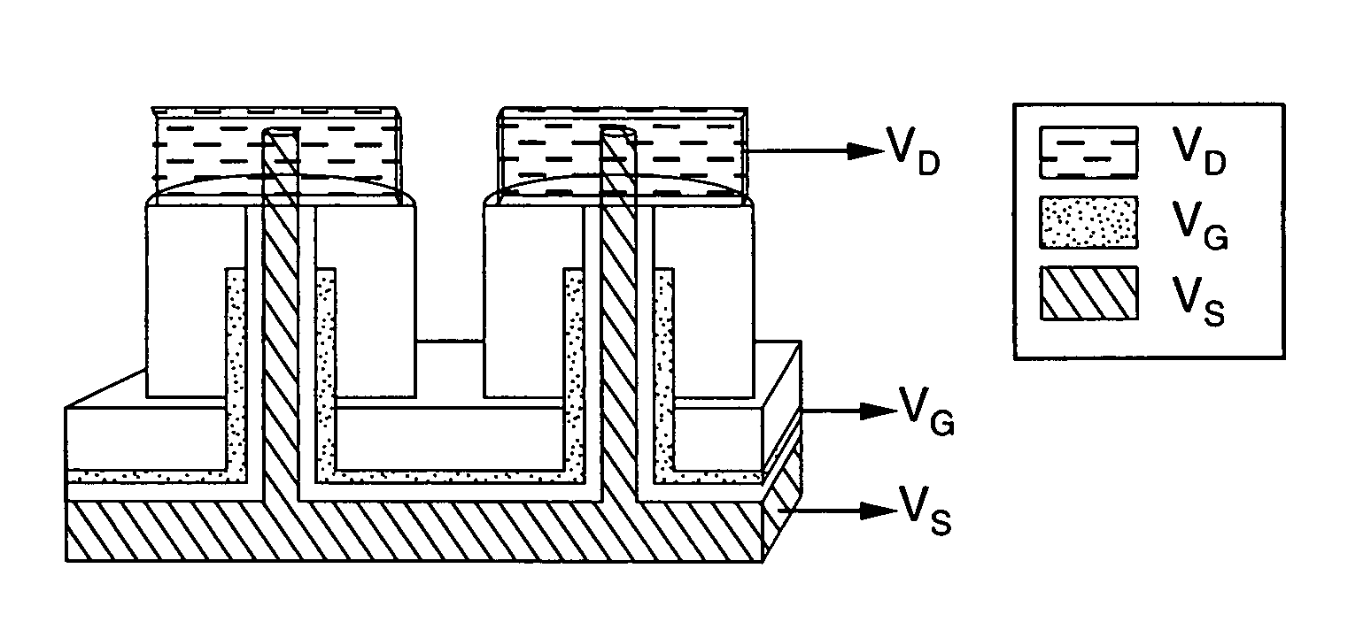
1. Silicon Nanowire Vertical integrated Surrounding-Gate FET.

[0074]As semiconductor devices are scaled into the sub 50 nm regime, short-channel effects and poor sub-threshold characteristics begin to be problematic for traditional planar transistors. Novel vertical integrated surrounding gate field-effect transistor (FET) device geometries are described which provide enhanced performance, as defined by improvements in functional density, energy efficiency, scalability, and compatibility with CMOS, are required in order to push toward ever higher packing densities with ever ...


PUM

PropertyMeasurementUnit
sizeaaaaaaaaaa
lengthaaaaaaaaaa
diametersaaaaaaaaaa

Abstract

Vertical integrated field effect transistor circuits and methods are described which are fabricated from Silicon, Germanium, or a combination Silicon and Germanium based on nanowires grown in place on the substrate. By way of example, vertical integrated transistors are formed from one or more nanowires which have been insulated, had a gate deposited thereon, and to which a drain is coupled to the exposed tips of one or more of the nanowires. The nanowires are preferably grown over a surface or according to a desired pattern in response to dispersing metal nanoclusters over the desired portions of the substrate. In one preferred implementation, SiCl4 is utilized as a gas phase precursor during the nanowire growth process. In place nanowire growth is also taught in conjunction with structures, such as trenches, while bridging forms of nanowires are also described.

Description

CROSS-REFERENCE TO RELATED APPLICATIONS[0001]This application claims priority from, and is a 35 U.S.C. §111(a) continuation of, co-pending PCT international application serial number PCT / US2006 / 032153, filed on Aug. 16, 2006, incorporated herein by reference in its entirety, which claims priority from U.S. provisional application Ser. No. 60 / 709,044 filed on Aug. 16, 2005, incorporated herein by reference in its entirety.[0002]This application is related to PCT International Publication No. WO 2007 / 022359 A2, published on 22 Feb. 2007, incorporated herein by reference in its entirety.STATEMENT REGARDING FEDERALLY SPONSORED RESEARCH OR DEVELOPMENT[0003]This invention was made with Government support under Grant No. DE-FG02-02ER46021, awarded by the Department of Energy. The Government has certain rights in this invention.INCORPORATION-BY-REFERENCE OF MATERIAL SUBMITTED ON A COMPACT DISC[0004]Not ApplicableNOTICE OF MATERIAL SUBJECT TO COPYRIGHT PROTECTION[0005]A portion of the materi...

Claims


Application Information

Patent Timeline
Patent Type & Authority Applications(United States)
IPC IPC(8): H01L29/08H01L21/336H01L29/78B82Y40/00B82Y99/00
CPCB82Y10/00H01L27/1292H01L21/84H01L27/1203H01L29/045H01L29/0665H01L29/0673H01L29/0676H01L29/42392H01L29/66772H01L29/78642H01L29/78684H01L29/78687H01L29/78696H01L21/823487
Inventor YANG, PEIDONGGOLDBERGER, JOSHUAHOCHBAUM, ALLONFAN, RONGHE, RONGRUI
Owner RGT UNIV OF CALIFORNIA
Why Eureka
Try Eureka