Substrate for light-emitting element and light-emitting device

a technology of light-emitting elements and substrates, which is applied in the direction of solid-state devices, printed circuit aspects, circuit thermal arrangements, etc., can solve the problems of insufficient emission brightness, high cost of raw materials, and insufficient thermal conductivity of alumina substrates, so as to achieve sufficient heat generation of light-emitting elements, sufficient emission brightness, and sufficient heat dissipation properties

Inactive Publication Date: 2011-09-29
ASAHI GLASS CO LTD
View PDF6 Cites 17 Cited by
  • Summary
  • Abstract
  • Description
  • Claims
  • Application Information

AI Technical Summary

Benefits of technology

[0020]By the substrate for light-emitting element of the present invention, it is possible to sufficiently dissipate heat generation of a light-emitting element solely by a heat dissipation layer in parallel with a light-emitting element-mounting surface of the substrate, which is economically advantageous as compared with thermal vias. Further, by using the substrate for light-emitting element of the present invention, it is possible to obtain a suff

Problems solved by technology

However, along with a tendency to high brightness of a light-emitting diode element, heat generation is also increasing, and the temperature increases excessively, whereby adequate emission brightness has not necessarily been obtainable.
However, the thermal conductivity of the alumina substrate is not necessarily high at a level of from about 15 to 20 W/m·K.
However, the aluminum nitride substrate has drawbacks such that the cost of raw materials is high, and it is hardly sintered, whereby high temperature firing will be required, thus leading to an increase in the process cost.
Further, the thermal expansion coefficient of the aluminum nitride substrate is as small as 4×10⁻⁶ to 5×10⁻⁶/° C., and when it is mounted on a printed substrate having a thermal expansion coefficient of at least 9×10⁻⁶/° C. as a universal product, adequate connection reliability cannot necessarily be obtainable due to the differen

Method used


Image

  • Substrate for light-emitting element and light-emitting device
  • Substrate for light-emitting element and light-emitting device
  • Substrate for light-emitting element and light-emitting device

Examples


first embodiment

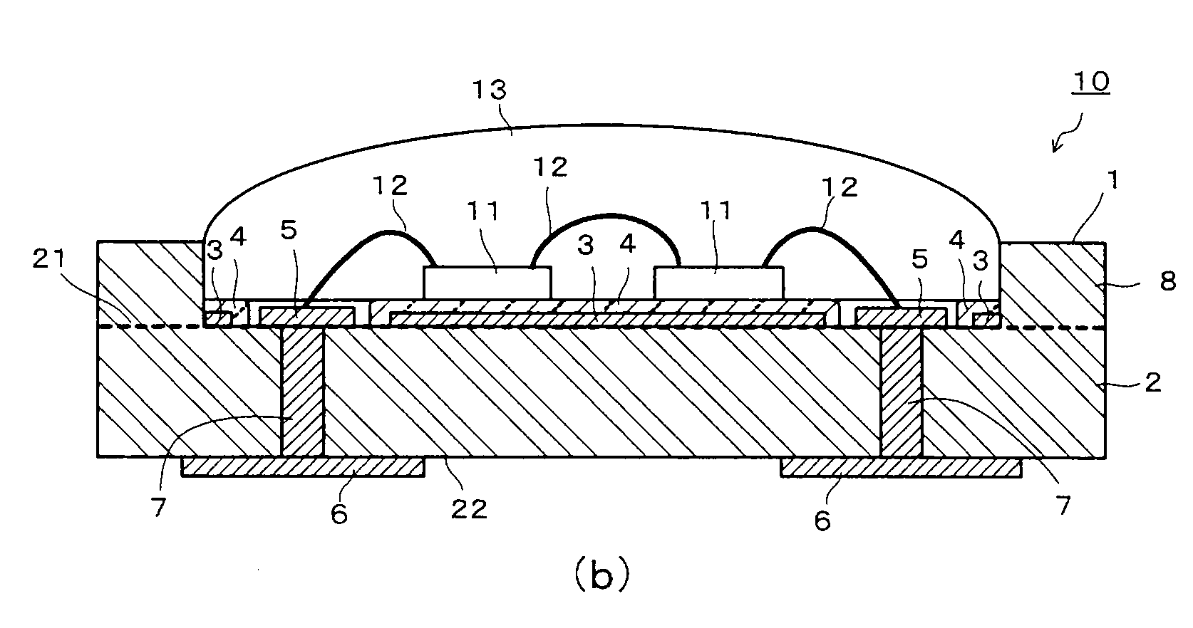
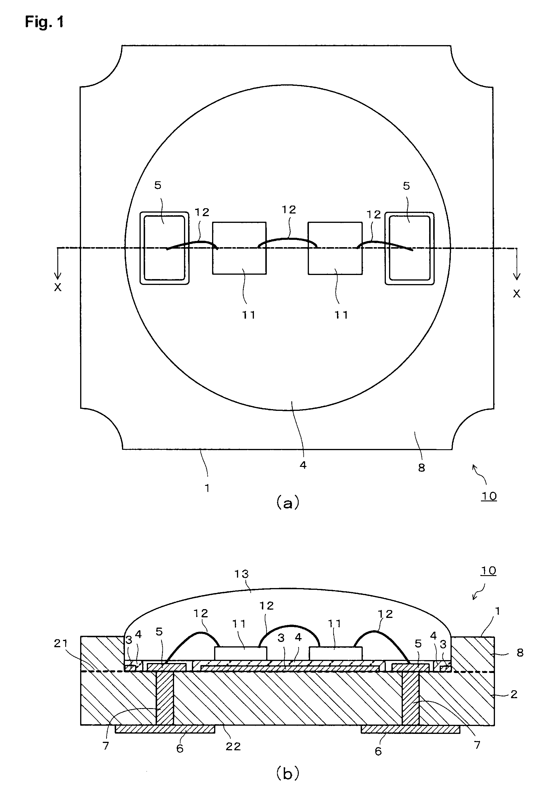
[0032]FIG. 1 is a plan view (a) illustrating an example of the substrate 1 for light-emitting element according to the first embodiment of the present invention and the light-emitting device 10 employing it, and a cross-sectional view (b) along its X-X line.

[0033]On the substrate 1 for light-emitting element of the present invention, for example, as shown in FIG. 1, two light-emitting elements 11 are mounted so that they are electrically connected in series. This substrate 1 for light-emitting element is used for a light-emitting device 10 wherein light-emitting elements 11 are electrically connected in series by bonding wires 12, and a sealing layer 13 is provided to cover these light-emitting elements 11 and the bonding wires 12. That is, in the light-emitting device 10 shown in FIG. 1, the portion excluding the light-emitting elements 11, the bonding wires 12 and the sealing layer 13, is the substrate 1 for light-emitting element of the present invention.

[0034]Here, the first emb...

second embodiment

[0095]Now, a second embodiment of the present invention will be described wherein as an insulating protective layer, a layer of a sintered product of a second glass ceramics composition comprising a glass powder and a ceramics filler is used.

[0096]FIG. 4 is a plan view (a) illustrating an example of the substrate 1 for light-emitting element according to the second embodiment of the present invention and the light-emitting device 10 employing it, and a cross-sectional view (b) along its X-X line.

[0097]The substrate 1 for light-emitting element of the present invention is one wherein, for example, as shown in FIG. 4, two light-emitting elements 11 are to be mounted so that they are electrically connected in series. This substrate 1 for light-emitting element is used as a light-emitting device 10 wherein light-emitting elements 11 are electrically connected in series by bonding wires 12, and a sealing layer 13 is provided to cover such light-emitting elements 11 and bonding wires 12. ...

example 1

[0138]By the following process, a light-emitting device for test having the same construction as shown in FIG. 4 was prepared. Here, in the same manner as above, the same symbols are used for the components before and after the firing.

[0139]Firstly, a green sheet 2 for main body to prepare the substrate main body 2 of the substrate 1 for light-emitting element, a green sheet 4 for insulating protective layer and a green sheet 8 for frame member were prepared. For each green sheet, raw materials were blended and mixed so that SiO2 became 60.4 mol %, B2O3 15.6 mol %, Al2O3 6 mol %, CaO 15 mol %, K2O 1 mol % and Na2O 2 mol %, and this raw material mixture was put into a platinum crucible and melted at 1,600° C. for 60 minutes. Then, this molten state glass was cast and cooled. This glass was ground by a ball mill made of alumina for 40 hours to obtain a glass powder for the substrate main body. Here, ethyl alcohol was used as the solvent at the time of grinding.

[0140]40 mass % of this ...


PUM


Abstract

To provide a substrate for light-emitting element, which is capable of sufficiently dissipating heat generation of a light-emitting element solely by a heat dissipation layer disposed in parallel with a light-emitting element-mounting surface of the substrate, which is economically advantageous as compared with thermal vias.
A substrate for light-emitting element, which comprises a substrate main body made of a sintered product of a first glass ceramics composition comprising a glass powder and a ceramics filler, wherein a surface on the side where a light-emitting element is to be mounted, is regarded as its main surface, and parts of wiring conductors for electrically connecting electrodes of the light-emitting element and an external circuit, are provided on the main surface; a heat dissipation layer formed on the substrate main body in such a shape to exclude said parts of wiring conductors and the vicinity around them and the periphery of the main surface, made of a metal material containing silver, having a thickness of from 8 to 50 μm and having a flat surface; and an insulating protective layer formed to cover the entirety of the heat dissipation layer including its edge and having a flat surface.

Description

TECHNICAL FIELD[0001]The present invention relates to a substrate for light-emitting element and a light-emitting device employing it, particularly to a substrate for light-emitting element having thermal resistance reduced and a light-emitting device employing it.BACKGROUND ART[0002]In recent years, along with a tendency to high brightness and whitening of a light-emitting diode element, a light-emitting device employing a light-emitting diode element has been used for backlights of mobile phones or liquid crystal TVs, liquid crystal displays, etc. However, along with a tendency to high brightness of a light-emitting diode element, heat generation is also increasing, and the temperature increases excessively, whereby adequate emission brightness has not necessarily been obtainable. Therefore, as a substrate for light-emitting element capable of mounting a light-emitting element such as a light-emitting diode element, one capable of readily dissipating heat generated from the light-...

Claims


Application Information

Patent Timeline
IPC IPC(8): H01L33/64
CPCH01L33/486H01L33/642H01L2924/10253H01L2224/48137H01L33/641H05K1/0203H05K1/0207H05K1/0306H05K2201/10106H01L2224/48091H01L2224/48227H01L2924/00014H01L2924/00H01L2924/181H01L2924/00012
Inventor NAKAYAMA, KATSUYOSHI
Owner ASAHI GLASS CO LTD
Why Eureka
Try Eureka