Light-emitting apparatus

a technology of light-emitting devices and auxiliary wiring lines, which is applied in the direction of electric lighting sources, electric light sources, solid-state devices, etc., can solve the problems of difficult widening the width of the auxiliary wiring lines formed on the same layer as the first electrode, affecting the efficiency of light-emitting devices, and reducing the resistance value of the second electrode to a desired value, etc., to achieve the effect of reducing shading, simple structure and low cos

Inactive Publication Date: 2011-10-06
CANON KK
View PDF1 Cites 8 Cited by
  • Summary
  • Abstract
  • Description
  • Claims
  • Application Information

AI Technical Summary

Benefits of technology

[0013]An object of the present invention is to reduce shading resulting from a voltage drop due to a resistance of a second electrode with an inexpensive and simple structure.
[0017]According to the present invention, organic light-emitting diode devices each having a cathode terminal connected to a common electrode and organic light-emitting diode devices each having an anode terminal connected to the common electrode are arranged alternately to coexist. This causes a differential current to flow in the common electrode, thereby reducing the voltage drop.
[0018]The amount of current supplied to the common electrode is small, and thus a line width of a current supply wiring line disposed at the outer periphery of the display region may be made thinner, and the organic EL device panel may accordingly have a narrower frame width.
[0019]Unlike the conventional methods of preventing shading, the present invention does not need to lower the resistance value of the common electrode or of a line for supplying current to the common electrode.

Problems solved by technology

However, there arises a problem that twisting or warping of a shadow mask used for the evaporation breaks a pattern of the auxiliary wiring line or makes the width of the auxiliary wiring line nonuniform.
However, widening the wiring width of the auxiliary wiring line that is formed on the same layer as the first electrode is difficult because of limited dimensions allocated to the auxiliary wiring line.
When the display screen size is large, in particular, the lengthened auxiliary wiring line raises the resistance value, whereby the resistance value of the second electrode may not be lowered to a desired value.
Lowering the resistance of the second electrode with the use of the auxiliary wiring line thus presents difficulties in terms of precision as well as production steps, and has not succeeded in completely preventing shading.

Method used


Image

  • Light-emitting apparatus
  • Light-emitting apparatus
  • Light-emitting apparatus

Examples


first embodiment

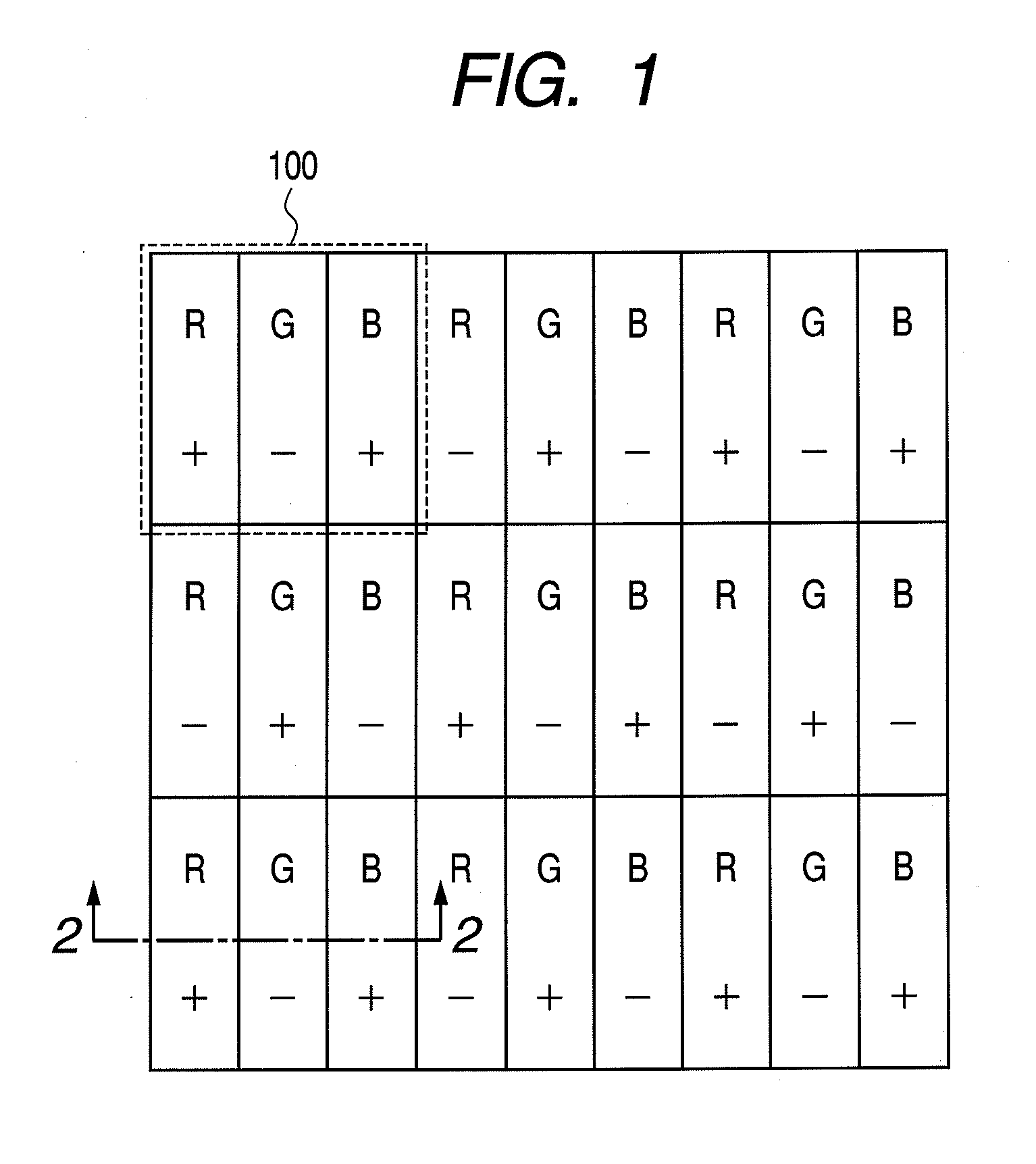
[0030]FIG. 1 illustrates an example in which a light-emitting apparatus according to a first embodiment of the present invention is used as a display. A pixel 100 is composed of three subpixels, R, G, and B, which include organic EL light-emitting devices of three different colors, red (R), green (G), and blue (B), respectively.

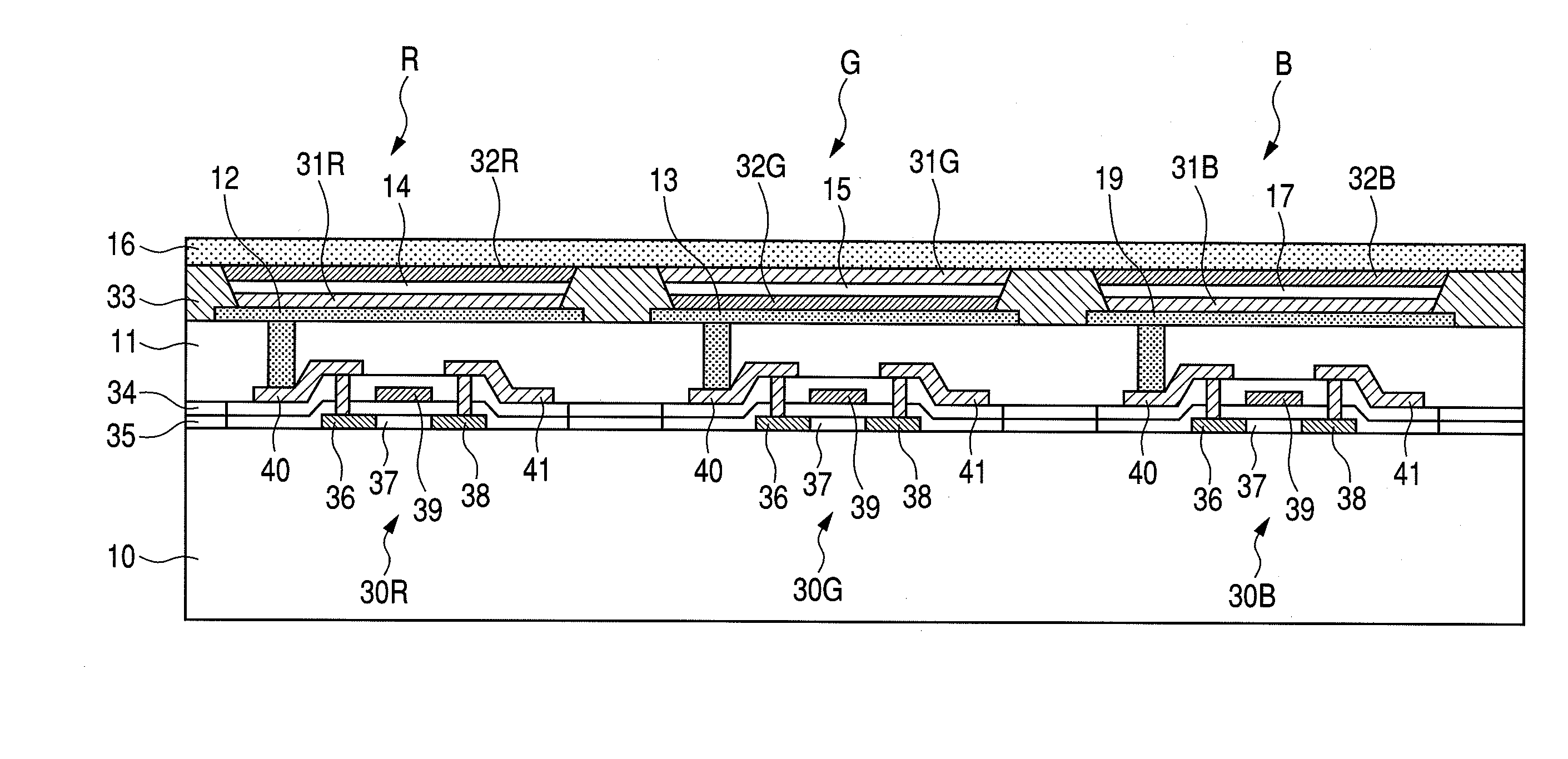
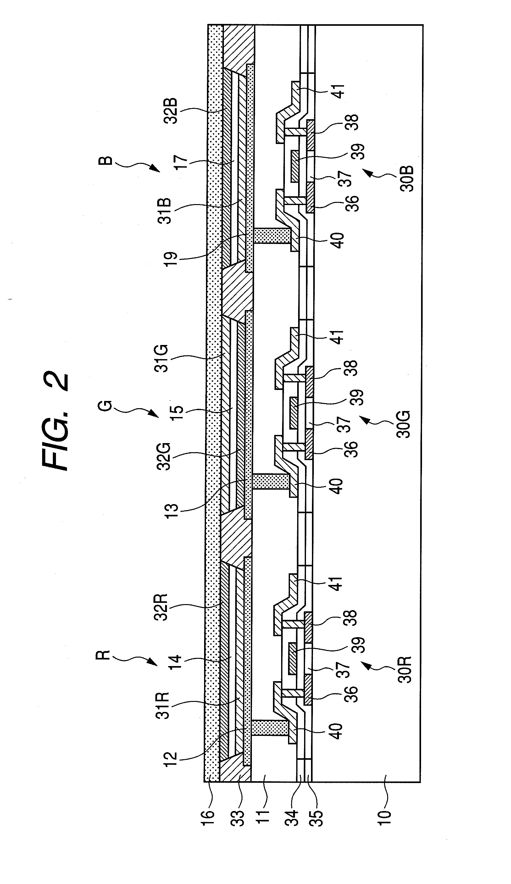
[0031]FIG. 2 is a cross-sectional view of a single pixel 100 taken along line 2-2 of FIG. 1.

[0032]The R subpixel is driven by a thin film transistor (TFT) 30R. The R subpixel includes, on a lower electrode 12 connected to a drain electrode 40 of the TFT 30R, a hole injection layer 31R, a light emission layer 14, and an electron injection layer 32R which are stacked in the mentioned order and covered with an upper electrode 16.

[0033]The G subpixel next to the R subpixel is driven by a thin film transistor (TFT) 30G. The G subpixel includes, on a lower electrode 13 connected to a drain electrode 40 of the TFT 30G, an electron injection layer 32G, a light emissi...

second embodiment

[0051]A pixel arrangement of FIG. 4 is a modification of the first embodiment in which the three subpixels R, G, and B of the pixel 100 have such layer structures that set the direction of a certain direction current ((+) connection or (−) connection) of one subpixel reverse to that of its adjacent subpixel, while the direction of the certain direction current ((+) connection or (−) connection) of a subpixel of one color in a pixel is identical to that of a subpixel of the same color in its adjacent pixel. In FIG. 4, the G light-emitting device alone is connected in the (−) direction whereas the R and B light-emitting devices are connected in the (+) direction.

[0052]This embodiment varies the direction in which an organic EL device is electrically connected to the common electrode (Vc) from one color to another. Organic EL devices separately applied with their color R, G, and B may thus exert the effects of the present invention without increasing organic EL film formation steps in ...

third embodiment

[0054]A subpixel arrangement according to a third embodiment of the present invention is illustrated in FIGS. 5A and 5B.

[0055]In this embodiment, the pixel 100 is formed of two subpixels 100a and 100b, which emit light of two different colors at different points in time. FIGS. 5A and 5B illustrate the colors of light that the subpixels 100a and 100b emit in two different subfields. Those two subfields are actually combined into one frame of image.

[0056]The subpixel 100a emit red (R) light and blue (B) light alternately. The subpixel 100b emit green (G) light and blue (B) light alternately. The subpixels 100a and 100b are arranged in a fixed pattern, and the pattern is cyclically repeated in the row direction and the column direction.

[0057]In the example of FIGS. 5A and 5B, the subpixel 100a and subpixel 100b of a single pixel take turns in emitting blue light. The pixels 100a and 100b do not emit red light and green light in combination, and do not emit blue light simultaneously.

[00...


PUM


Abstract

Provided is a light-emitting apparatus including a plurality of light-emitting devices arranged on a substrate, the plurality of light-emitting devices each including a pair of electrodes and an organic emission layer which is interposed between the pair of electrodes with one of the pair of electrodes serving as an anode and another one of the pair of electrodes serving as a cathode, wherein one of the pair of electrodes is an electrode common to the plurality of light-emitting devices, and wherein, of the plurality of light-emitting devices, ones that have the common electrode as their anodes and ones that have the common electrode as their cathodes are arranged alternately.

Description

TECHNICAL FIELD[0001]The present invention relates to a light-emitting apparatus including light-emitting devices, specifically, organic electroluminescent devices.BACKGROUND ART[0002]Electroluminescence (hereinafter simply referred to as EL) of an organic material is used in an organic EL device in which an organic layer is interposed between a first electrode and a second electrode. The organic EL devices are attracting attention as a light-emitting device capable of emitting light of a high luminance while driven at low voltage. A light-emitting apparatus with organic EL devices arranged in a matrix pattern on a substrate is used as a display apparatus.[0003]A self-emission type display apparatus that uses an organic EL device as described above (namely, organic EL display) includes a thin film transistor (hereinafter referred to as TFT) in each pixel on a substrate. The TFT is covered with an interlayer insulating film on which the organic EL device is formed. The organic EL dev...

Claims


Application Information

Patent Timeline
Patent Type & Authority Applications(United States)
IPC IPC(8): H01L27/15H05B44/00
CPCH01L27/32H01L51/5203H01L27/3276H01L27/3211H10K59/35H10K59/00H10K59/131H10K59/805H10K50/805
Inventor YOSHINAGA, HIDEKIMORI, HIDEO
Owner CANON KK
Why Eureka
Try Eureka