

Structure for self-aligned silicide contacts to an upside-down fet by epitaxial source and drain
a technology of fet and contact, applied in the field of microelectronics, can solve the problems of failure, unwanted capacitance, and failure of back-side contacts to the source and drain, and achieve the effect of inducing strain in the channel region
- Summary
- Abstract
- Description
- Claims
- Application Information
AI Technical Summary
Benefits of technology
Problems solved by technology
Method used
Image

Examples
Embodiment Construction
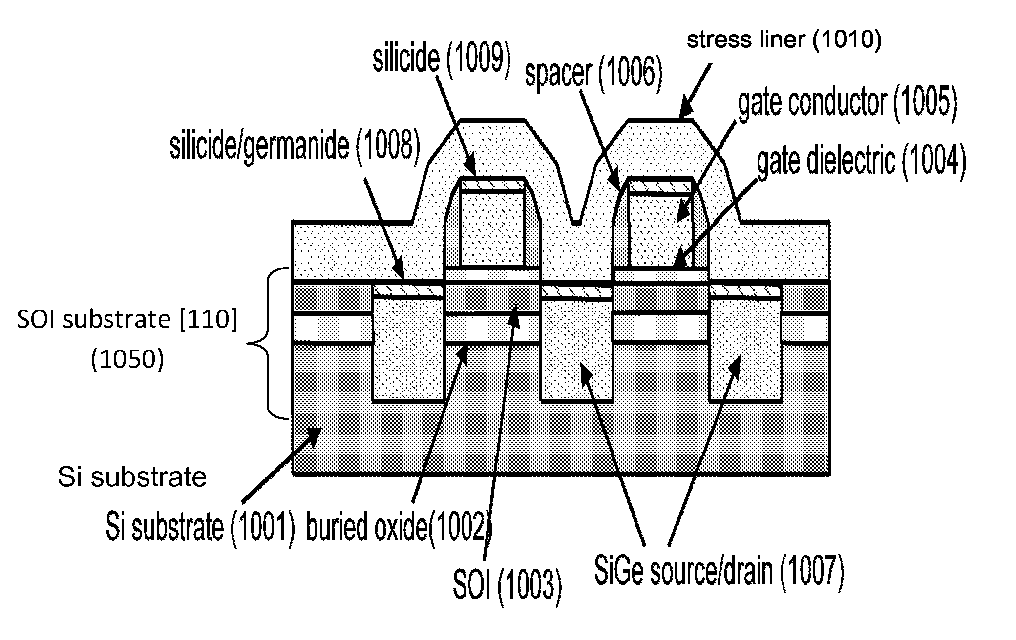
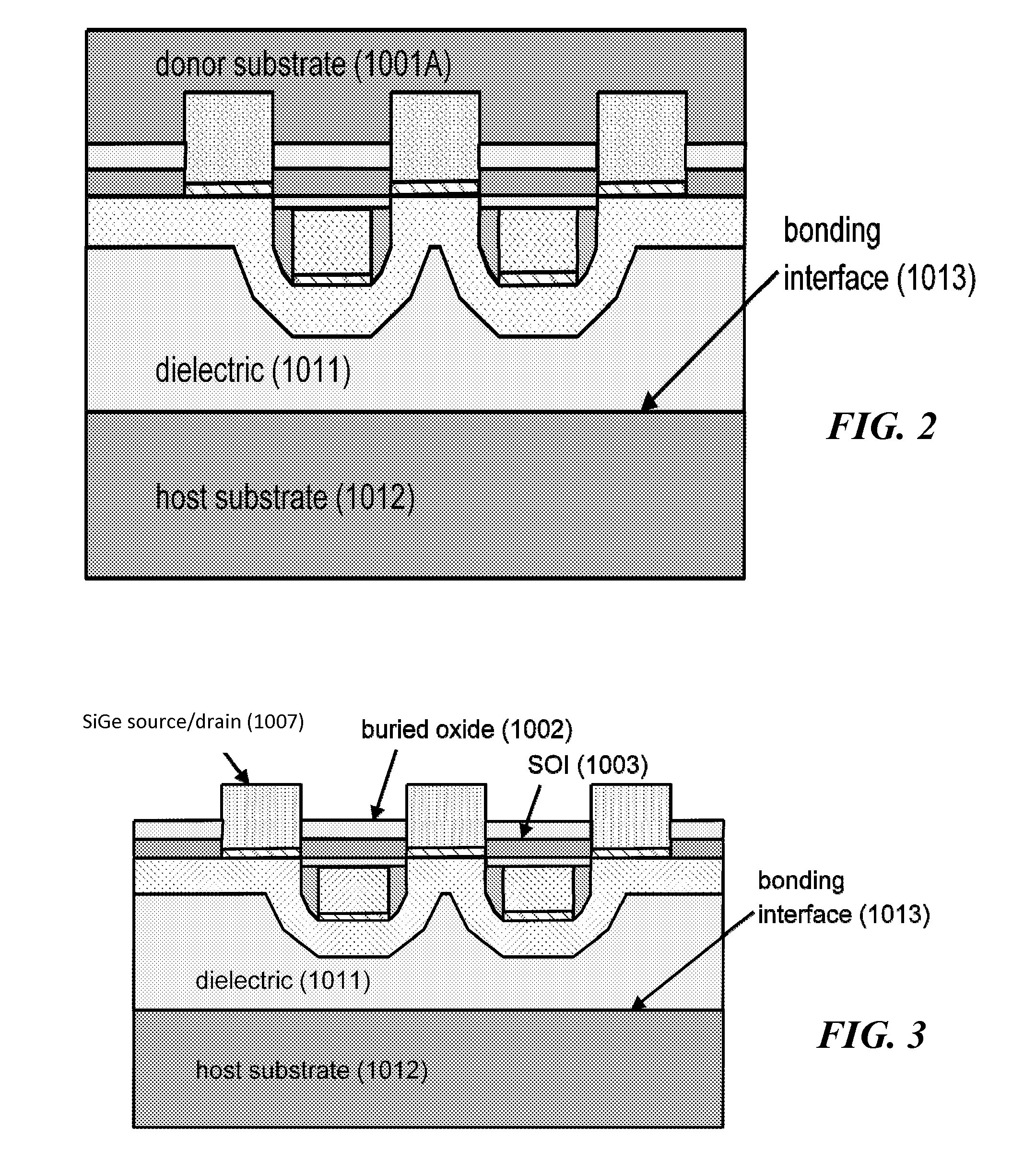
[0023]We describe an improved design structure and method to form field-effect transistors for semiconductors using self-aligned silicide contacts to the back-side of the source and drain regions, thus eliminating the need to form contact holes through the source and drain region. More specifically, the design includes self-aligned silicide / germanide (SiGe) ohmic contacts formed over the epitaxial SiGe source / drain regions of upside-down field-effect transistors. An ohmic contact is a contact between two materials which exhibit a linear and symmetric current-voltage (I-V) curve. In the following discussion “front-side” refers to the surface on which the integrated circuit devices are made prior to flipping over the FET, and “back-side” refers to the surface that is to become the top surface after the device is turned over.
[0024]An upside-down FET (UFET) according to the invention reduces the parasitic capacitance between the gate conductor line and the metal filled via that forms a ...
PUM
 Abstract
Description
Claims
Application Information