
Magnetoresistive random access memory element and fabrication method thereof

a random access and memory element technology, applied in the direction of inductance/transformer/magnet manufacturing, magnetic bodies, instruments, etc., can solve the problem of insufficient strength to switch the magnetization in the reference layer, limiting cell sizes, and affecting the gap filling process of the reference layer using physical vapor deposition methods

Active Publication Date: 2011-10-06
NAN YA TECH
View PDF11 Cites 46 Cited by
  • Summary
  • Abstract
  • Description
  • Claims
  • Application Information

AI Technical Summary

Benefits of technology

[0002]The present invention relates generally to the filed of non-volatile memory technology. More particularly, the present invention relates to a magnetoresistive random access memory (MRAM) element with improved magnetization efficiency, and method for fabricating the same.

Problems solved by technology

The reference layer usually is composed of a magnetic material in which the magnetization is pinned so that the magnetic field, which is applied to the data layer and in part penetrates the reference layer, is of insufficient strength to switch the magnetization in the reference layer.
However, the most basic MRAM cell suffers from the half-select problem, which limits cell sizes.
However, the prior art MRAM has several drawbacks.
For example, the gap fill process of the reference layer using physical vapor deposition (PVD) methods becomes problematic when the aspect ratio of the gap is greater than 2 for example.
Besides, as the cell packing density increases, the interference between neighboring cells is not negligible.

Method used


Image

  • Magnetoresistive random access memory element and fabrication method thereof
  • Magnetoresistive random access memory element and fabrication method thereof
  • Magnetoresistive random access memory element and fabrication method thereof

Examples


Embodiment Construction

[0017]In the following description, numerous specific details are given to provide a thorough understanding of the invention. However, it will be apparent to one skilled in the art that the invention may be practiced without these specific details. In order to avoid obscuring the present invention, some well-known system configurations and process steps are not disclosed in detail.

[0018]Likewise, the drawings showing embodiments of the apparatus are semi-diagrammatic and not to scale and, particularly, some of the dimensions are for the clarity of presentation and are shown exaggerated in the figures. Also, in which multiple embodiments are disclosed and described having some features in common, for clarity and ease of illustration and description thereof, like or similar features will ordinarily be described with like reference numerals.

[0019]The term “horizontal” as used herein is defined as a plane parallel to the conventional major plane or surface of the semiconductor substrate...


PUM


Abstract

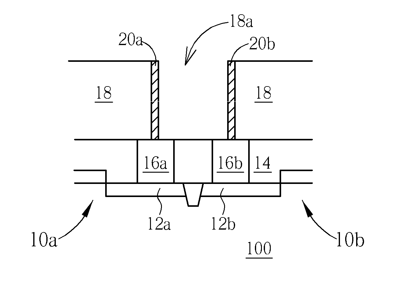
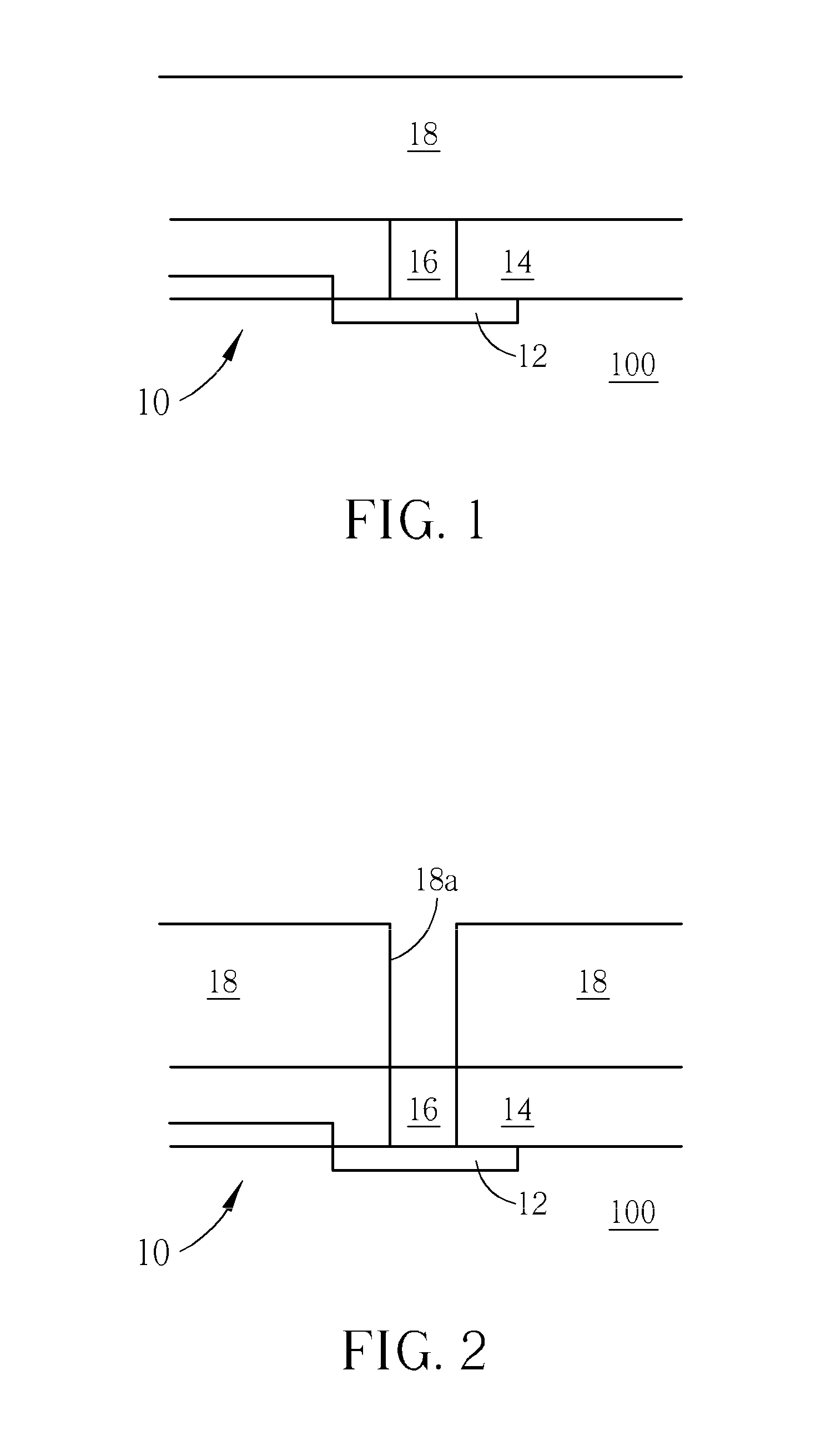
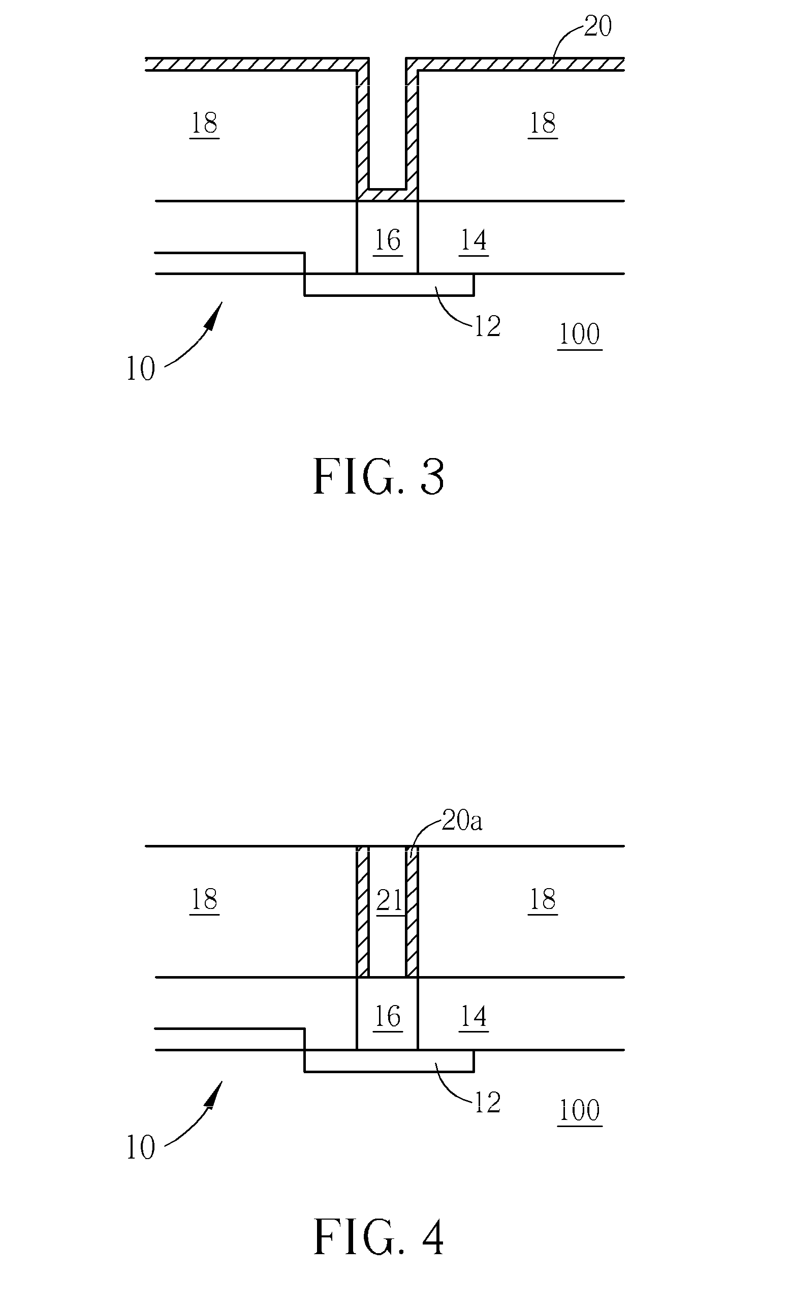
A magnetoresistive random access memory (MRAM) element includes a bottom electrode embedded in a first insulating layer; an annular reference layer in a first via hole of a second insulating layer on the first insulating layer, the annular reference layer being situated above the bottom electrode; a first gap fill material layer filling the first via hole; a barrier layer covering the annular reference layer, the second insulating layer and the first gap fill material layer; an annular free layer in a second via hole of a third insulating layer on the second insulating layer, the annular free layer being situated above the annular reference layer; and a top electrode stacked on the annular free layer.

Description

BACKGROUND OF THE INVENTION[0001]1. Field of the Invention[0002]The present invention relates generally to the filed of non-volatile memory technology. More particularly, the present invention relates to a magnetoresistive random access memory (MRAM) element with improved magnetization efficiency, and method for fabricating the same.[0003]2. Description of the Prior Art[0004]As known in the art, magnetoresistive random access memory (MRAM) is a non-volatile computer memory technology. MRAM is six times faster than the current industry-standard memory, dynamic RAM (DRAM). It is almost as fast as static RAM (SRAM) and is much faster and suffers less degradation over time than flash memory. Unlike these technologies, MRAM uses magnetism instead of electrical charges to store data.[0005]In general, the MRAM cells include a data layer and a reference layer. The data layer is composed of a magnetic material and during a write operation the magnetization of the data layer can be switched b...

Claims


Application Information

Patent Timeline
IPC IPC(8): H01L29/82H01L21/00
CPCB82Y25/00B82Y40/00H01F10/3254H01L43/10H01L43/08H01L43/12H01L43/02H01F41/308G11C11/161H10N50/01H10N50/10H10N50/80H10N50/85
Inventor HSIEH, CHUN-IWU, CHANG-RONG
Owner NAN YA TECH
Learn More