Amplifier circuit, signal processor circuit, and semiconductor integrated circuit device

a technology of signal processor and amplifier, which is applied in the direction of amplifier details, amplifier with semiconductor devices/discharge tubes, differential amplifiers, etc., to achieve the effect of increasing the circuit area

Inactive Publication Date: 2011-10-06
DENSO CORP
View PDF6 Cites 4 Cited by
  • Summary
  • Abstract
  • Description
  • Claims
  • Application Information

AI Technical Summary

Benefits of technology

[0007]It is an object of the present invention to provide an amplifier circuit having a function of switching its configuration between single end output configuration and differential output configuration without increasing a circuit area, a signal processor circuit including such an amplifier circuit, and a semiconductor integrated circuit device including such and amplifier circuit.

Problems solved by technology

This makes it unnecessary to change the specifications of the amplifier circuit according to the output method of the sensor.

Method used


Image

  • Amplifier circuit, signal processor circuit, and semiconductor integrated circuit device
  • Amplifier circuit, signal processor circuit, and semiconductor integrated circuit device
  • Amplifier circuit, signal processor circuit, and semiconductor integrated circuit device

Examples


first embodiment

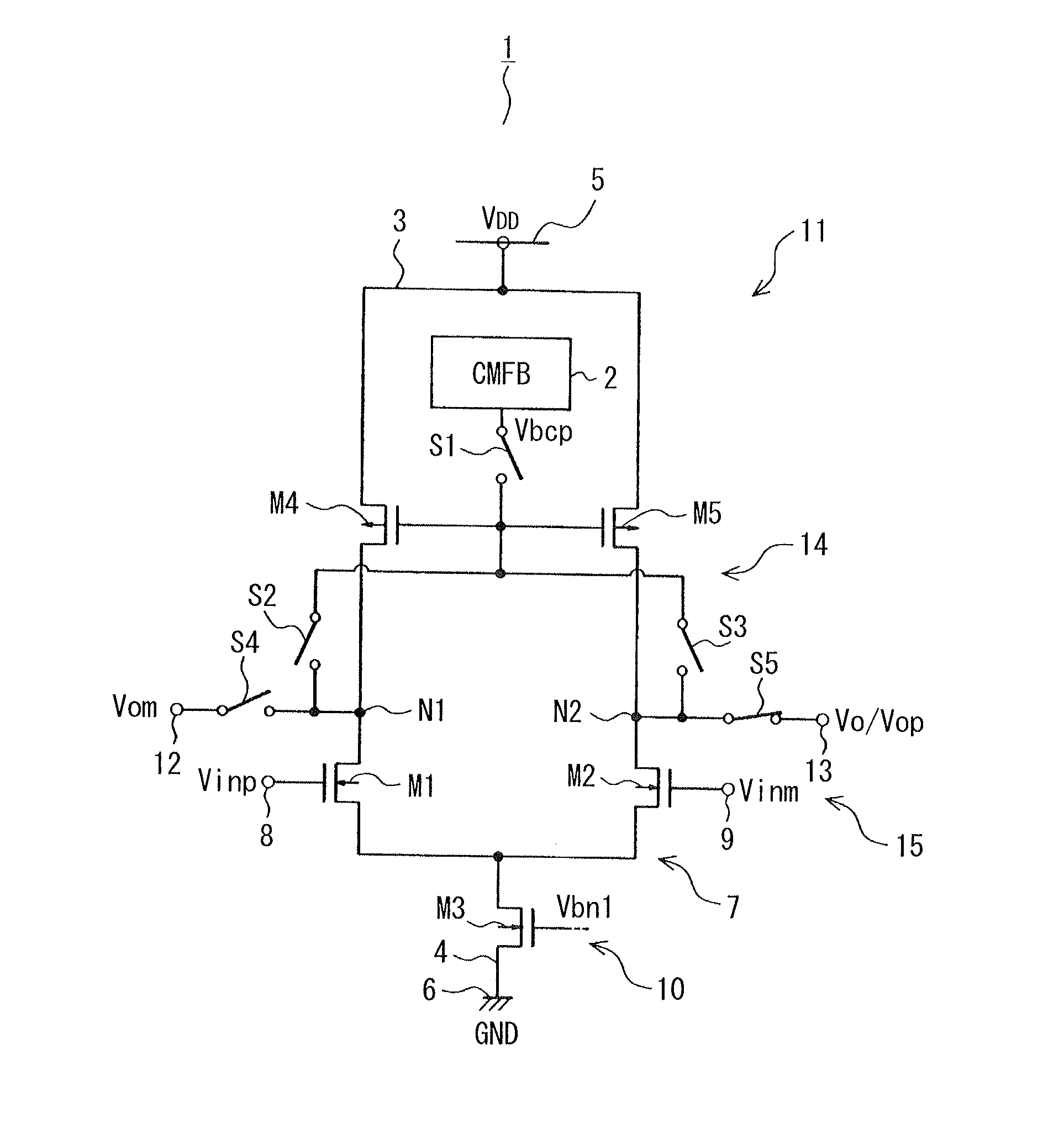
[0032]Referring to FIG. 1, an amplifier circuit 1 is used in a semiconductor integrated circuit device (IC) incorporated in, for example, an in-vehicle electronic control section (ECU). The amplifier circuit 1 includes MOS transistors M1 to M5, switches S1 to S5, and a common mode feedback (CMFB) circuit 2. Between power supply lines 3, 4, power supply voltage VDD (for example, 5V) is supplied through power supply terminals 5, 6.

[0033]N-channel MOS transistors M1, M2 (corresponding to differential input transistors) form a differential pair 7. Between the commonly connected source of the transistors M1, M2 and the power supply line 4, a n-channel MOS transistor M3 is connected. The gates of the transistors M1, M2 are respectively connected to an input terminal 8 (corresponding to a non-inverting input terminal) for input voltage Vinp and an input terminal 9 (corresponding to an inverting input terminal) for input voltage Vinm. To the gate of the transistor M3, appropriate (optimum) ...

second embodiment

[0097]A second embodiment of the present invention is shown in FIG. 13, which is equivalent to FIG. 1 referred to in relation to the first embodiment. The same elements as in the first embodiment will be indicated with the same reference numerals and the description thereof will be omitted.

[0098]An amplifier circuit 71 shown in FIG. 13 is different from the amplifier circuit 1 shown in FIG. 1 in that MOS transistors M71 to M75 are provided in place of the transistors M1 to M5 and a CMFB circuit 72 is provided in place of the CMFB circuit 2.

[0099]The p-channel MOS transistors M71, M72 (corresponding to differential input transistors) form a differential pair 73. Between the commonly connected source of the transistors M71, M72 and the power supply line 3, the p-channel MOS transistor M73 is connected. The gates of the transistors M71, M72 are respectively connected to the input terminals 8, 9. To the gate of the transistor M73, appropriate (optimum) bias voltage Vbp1 is applied. Thus...

third embodiment

[0104]A third embodiment of the present invention is shown in FIG. 14, which is equivalent to FIG. 1 referred to in relation to the first embodiment. The same elements as in the first embodiment will be marked with the same reference numerals and the description thereof will be omitted.

[0105]An amplifier circuit 81 shown in FIG. 14 is provided by changing the mode of the amplifier circuit 1 shown in FIG. 1 to folded cascode connection. The amplifier circuit 81 is different from the amplifier circuit 1 shown in FIG. 1 in that MOS transistors M81 to M88 are provided in place of the MOS transistors M4, M5 and a CMFB circuit 82 is provided in place of the CMFB circuit 2.

[0106]Between the power supply lines 3, 4, the following pairs of transistors are connected in series; n-channel transistors M81 and M82; n-channel transistors M83 and M84; p-channel transistors M85 and M86; and p-channel transistors M87 and M88. These transistors 81 to 88 are vertically stacked. Of these transistors, th...


PUM


Abstract

An amplifier circuit is provided to be switchable between a single end output configuration and a differential output configuration without increasing a circuit area. When first and fourth switches are turned off and a second switch is turned on, a load circuit functions as an active load on a differential pair and a first output terminal is internally disconnected. The amplifier circuit is provided with a single end output configuration and differentially amplifies input voltages inputted to input terminals and outputs an imbalanced signal from a second output terminal. When the first and fourth switches are turned on and the second switch is turned off, the load circuit functions as a load on the differential pair and the first output terminal is internally connected. The amplifier circuit is provided with a differential output configuration and differentially amplifies the input voltages inputted to the input terminals and outputs balanced signals from the output terminals.

Description

CROSS REFERENCE TO RELATED APPLICATION[0001]This application is based on and incorporates herein by reference Japanese patent application No. 2010-85151 filed on Apr. 1, 2010.FIELD OF THE INVENTION[0002]The present invention relates to an amplifier circuit that differentially amplifies and outputs signals inputted through differential input transistors in a differential pair, a signal processor circuit including the amplifier circuit, and a semiconductor integrated circuit device including the amplifier circuit.BACKGROUND OF THE INVENTION[0003]Of conventional capacitive sensors, for example, some are single end output type and the other of the capacitive sensors are differential output type. As for C-V converter circuits that convert sensor output signals into voltages, some are configured to use an amplifier circuit with a single end configuration and the other are configured to use an amplifier circuit with a differential configuration. (Refer to JP-2008-216135A, for example.) For...

Claims


Application Information

Patent Timeline
Patent Type & Authority Applications(United States)
IPC IPC(8): H03F3/45
CPCH03F3/45183H03F3/45192H03F3/45659H03F2200/261H03F2203/45404H03F2203/45421H03F2203/45728H03F2203/45434H03F2203/45512H03F2203/45514H03F2203/45544H03F2203/45726H03F2203/45424
Inventor HONDA, KAZUTAKAMAKIHARA, TETSUYAHORIE, MASAKIYO
Owner DENSO CORP
Why Eureka
Try Eureka