
Die structure and die connecting method

Inactive Publication Date: 2011-10-20
RAYDIUM SEMICON
View PDF3 Cites 0 Cited by
  • Summary
  • Abstract
  • Description
  • Claims
  • Application Information

AI Technical Summary

Benefits of technology

[0007]It is an object of the present invention to provide a die structure for electrically coupling to a circuit board at lower material cost.
[0008]It is another object of the present invention to provide a die connecting method at lower manufacture cost.

Problems solved by technology

It is difficult to reduce the manufacture cost due to the high price of the gold material.

Method used


Image

  • Die structure and die connecting method
  • Die structure and die connecting method
  • Die structure and die connecting method

Examples


Embodiment Construction

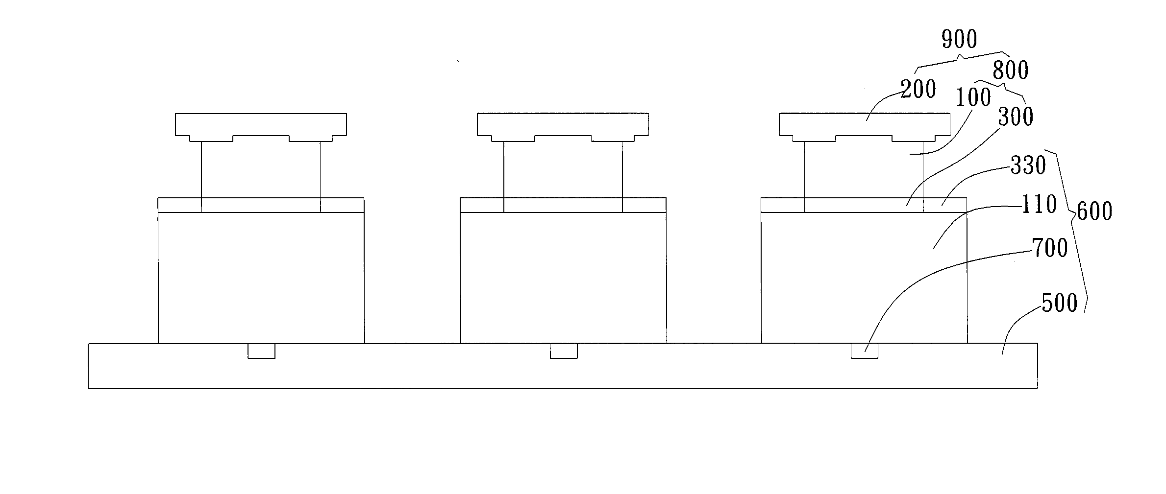
[0016]The present invention provides a die structure capable of being electrically coupled to a circuit board, wherein the circuit board includes a rigid or soft printed circuit board having various circuits. As shown in FIG. 2A, the die structure 900 of the present invention includes a die 200 and a bump structure 800, wherein the die 200 generally refers to an integrated circuit die. The bump structure 800 includes a body 100 and a solder layer 300. The body 100 is preferably disposed on the die 200. The solder layer 300 is disposed on the body 100. The solder layer 300 is conductive and melts down when being heated up to the melting point of the solder. In the preferred embodiment, the material of the solder layer 300 is tin, wherein the melting point of the solder is about 250° C. In other embodiments, however, the material of the solder layer 300 can be selected from the group consisting of tin-lead alloy, tin-silver alloy, and other metals or alloys. The material of the body 1...


PUM


Abstract

A die structure and a die connecting method using the same are provided. The die structure includes a die and a bump structure. The bump structure includes a body and a solder layer. The body is disposed on the die. The solder layer is disposed on the body. The method includes providing a die structure mentioned above, providing a circuit board mentioned above, and soldering the solder layer of the die structure with the tine layer on the copper block of the circuit board. In different embodiments, a tin layer is omitted from the circuit board, wherein the solder layer of the die structure is directly soldered onto the surface of the copper block.

Description

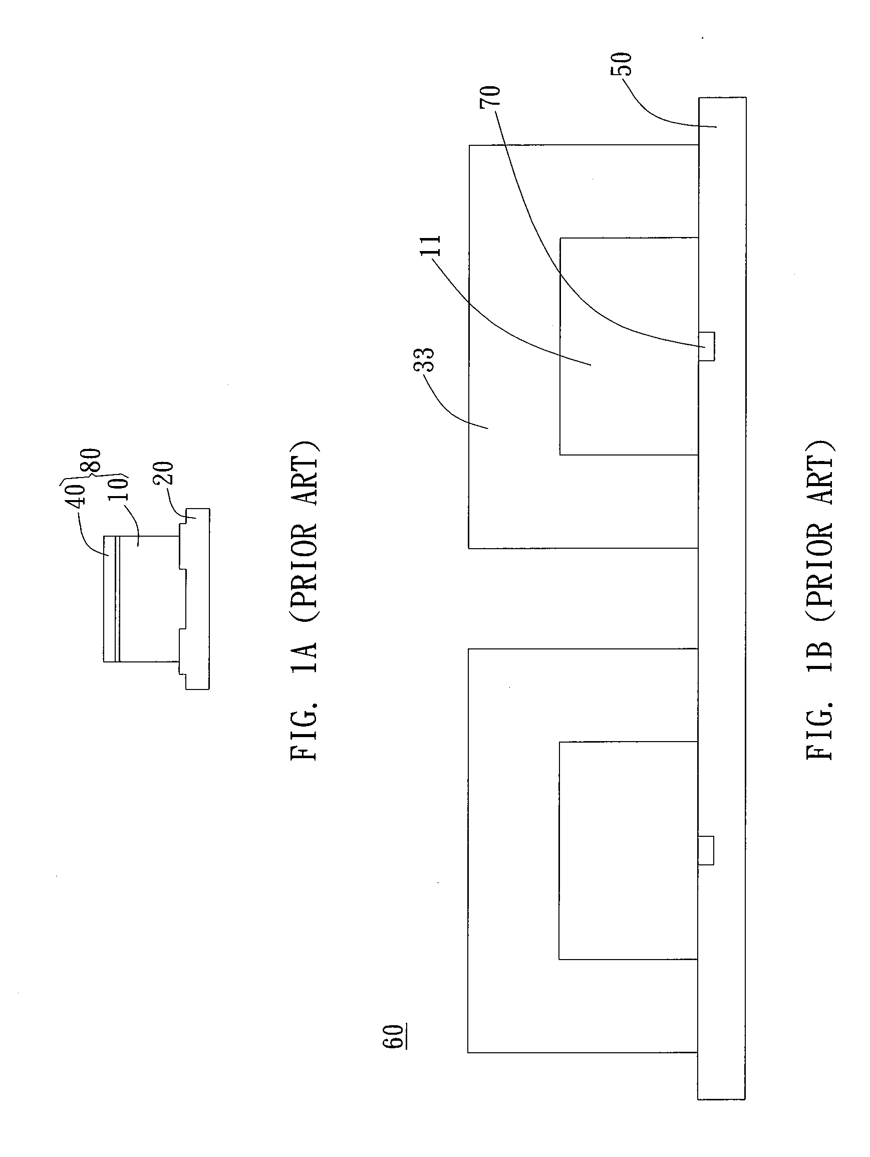
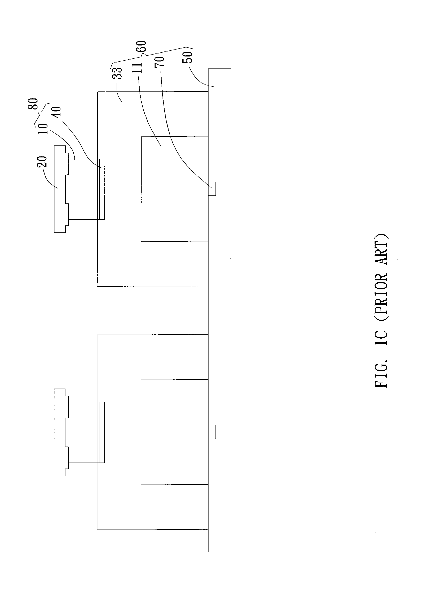
CROSS-REFERENCE TO RELATED APPLICATION[0001]This application claims priority based on Taiwanese Patent Application No. 099112293, filed on Apr. 20, 2010, the disclosure of which is incorporated herein by reference in its entirety.BACKGROUND OF THE INVENTION[0002]1. Field of the Invention[0003]This invention generally relates to a die structure and a die connecting method. More particularly, this invention relates to a die structure for electrically coupling to a circuit board and a die connecting method using the same.[0004]2. Description of the Prior Art[0005]Among the chip-packaging technologies, flip-chip interconnect technology (FC) is generally used. In the flip-chip interconnect technology, a plurality of die pads are disposed in area array on an active surface of the die, wherein a bump structure 80 shown in FIG. 1A is formed on the die pad. After flipping the die 20, the bump structure 80 on the die 20 is coupled to a circuit 70 in the circuit board 60 shown in FIG. 1B via a...

Claims


Application Information

Patent Timeline
IPC IPC(8): H01L23/485H01L21/58
CPCH01L24/13H01L2924/00013H01L24/81H01L2224/1308H01L2224/13082H01L2224/13111H01L2224/13147H01L2224/13562H01L2224/13564H01L2224/1357H01L2224/13611H01L2224/13644H01L2224/8101H01L2224/81193H01L2224/81801H01L2924/01029H01L2924/01079H01L2924/01082H01L24/16H01L2924/01006H01L2924/01033H01L2924/01047H01L2924/014H01L2924/0105H01L2924/00015H01L2924/00014H01L2224/13099H01L2924/14H01L2924/00
Inventor HSU, CHIA-HUNGLIN, CHING-SANCHEN, CHIN-YUNG
Owner RAYDIUM SEMICON
Learn More