Image acquisition system and method for the manufacture thereof
a technology of image acquisition and acquisition system, applied in the field of image acquisition system, can solve the problems of laborious assembly and adjustment, relatively complex construction,
- Summary
- Abstract
- Description
- Claims
- Application Information
AI Technical Summary
Benefits of technology
Problems solved by technology
Method used
Image
Examples
Embodiment Construction
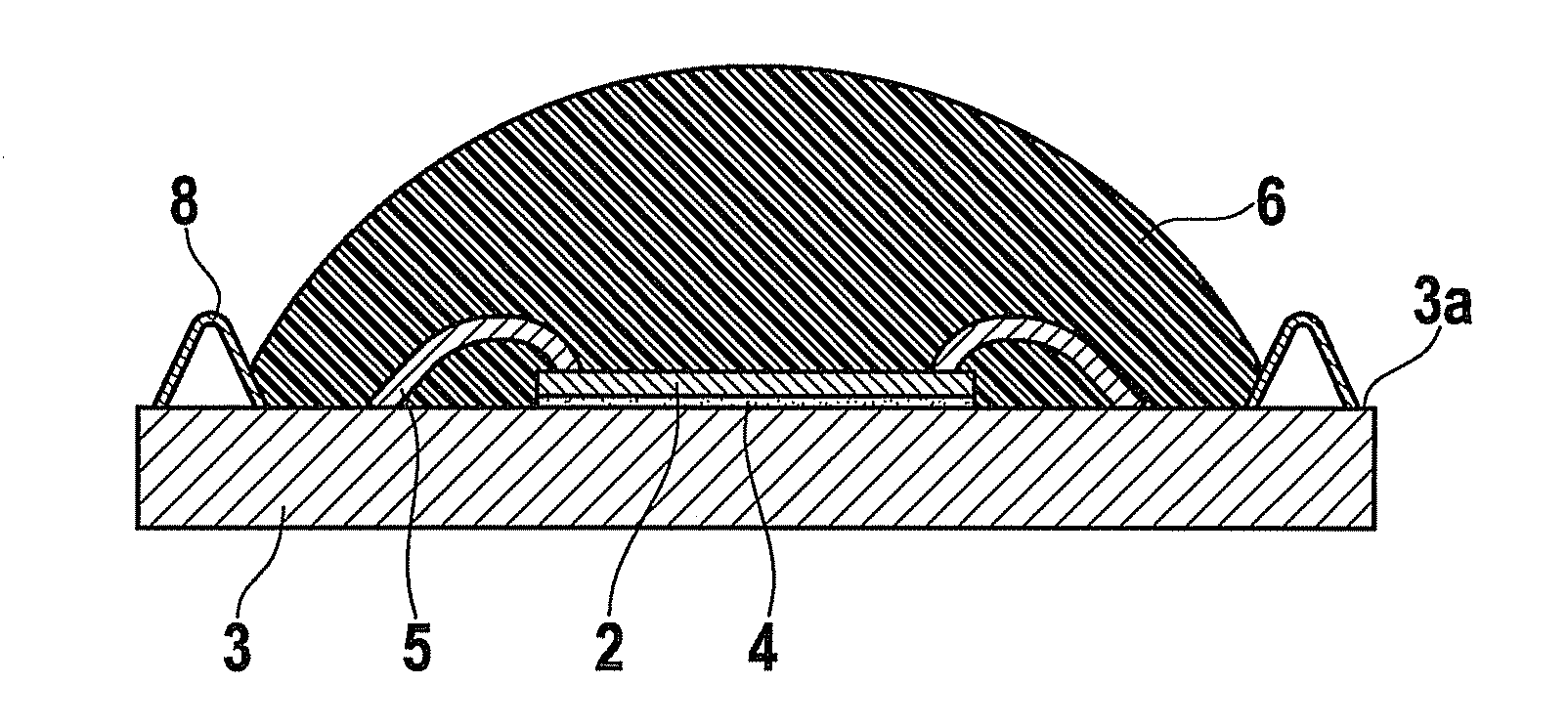
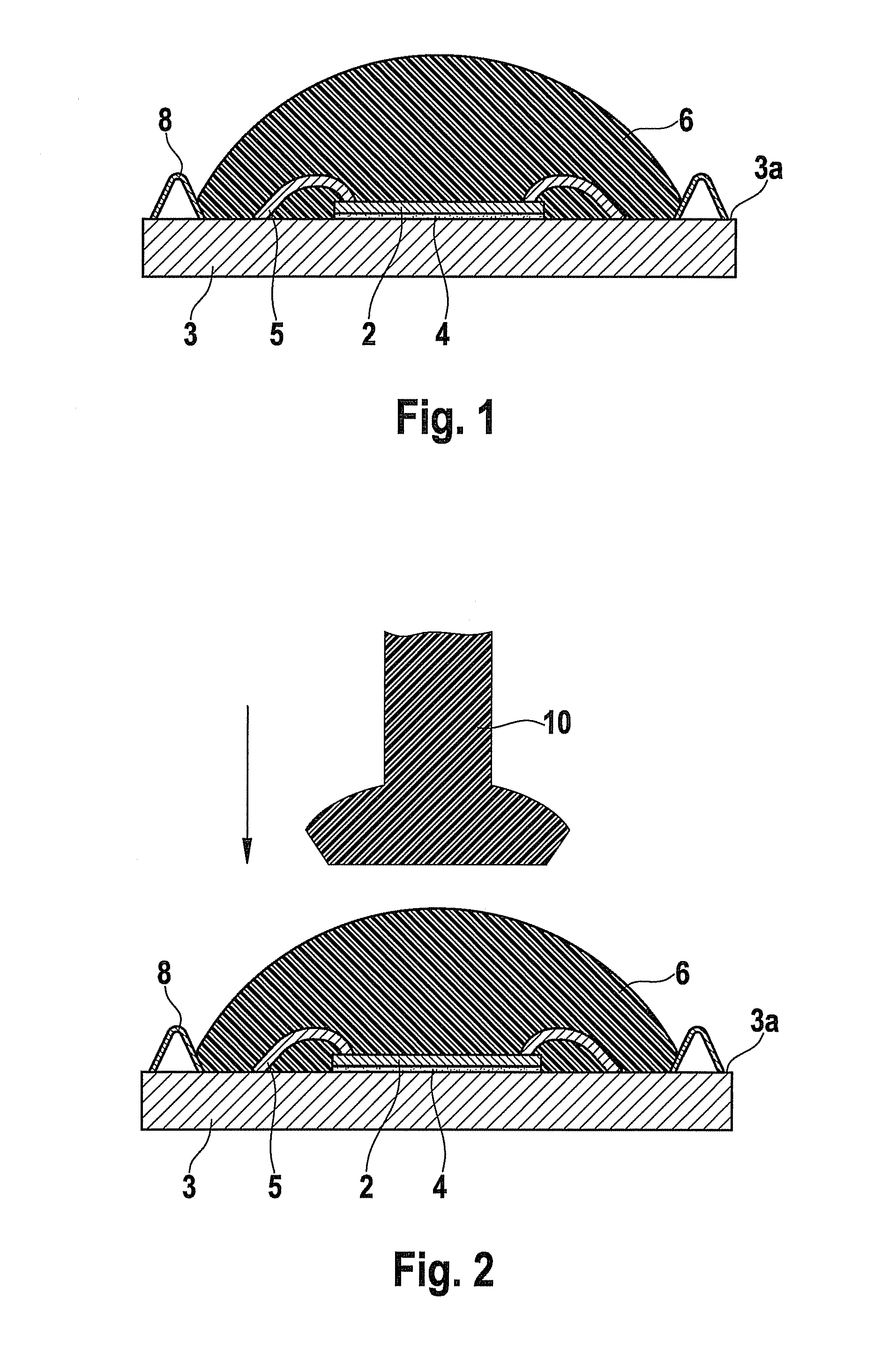
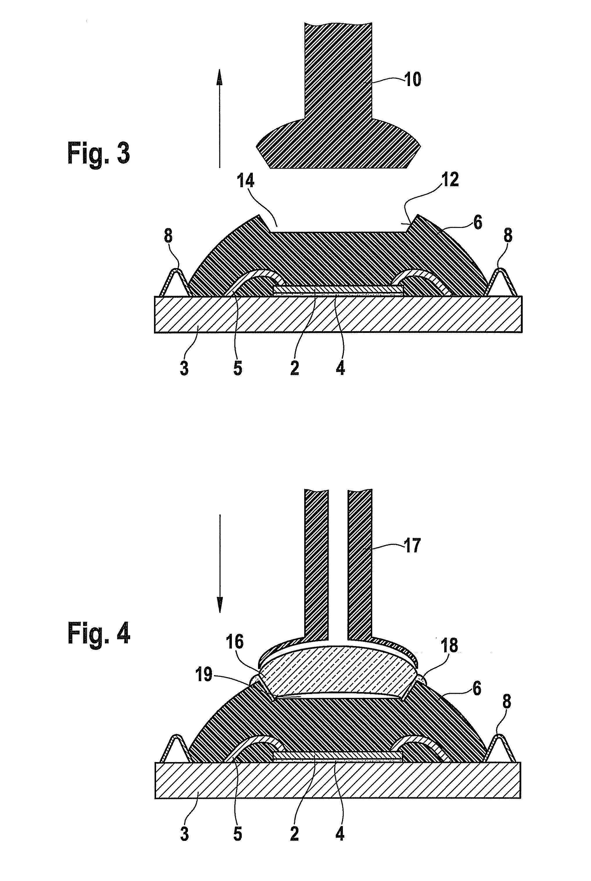
[0020]In order to manufacture an image acquisition system 1 shown in FIG. 5, according to FIG. 1 firstly an imager chip 2 constituting an image sensor is secured on upper substrate side 3a of a substrate 3, e.g. a circuit board 3, by way of, for example, an adhesive layer 4, and is contacted via bonding wires 5. A sealing compound (glob top) is then applied onto upper substrate side 3a such that it completely covers imager chip 2 and its wire bonds 5. A delimiter 8 for delimiting the applied sealing compound 6 is advantageously provided on upper substrate side 3a. Delimiter 8 can be embodied, as shown in FIG. 1, in particular by a rim 8 configured peripherally, i.e. in particular annularly, on substrate 3. Also possible, however, are stop edges at which excess material is discharged to the side in the event of an overflow.
[0021]As shown in FIG. 1, sealing compound 6 is advantageously applied in liquid or viscous or pasty fashion in a convex shape, e.g. droplet shape, which is promot...
PUM
| Property | Measurement | Unit |
|---|---|---|
| Transparency | aaaaa | aaaaa |
Abstract
Description
Claims
Application Information


