Semiconductor device and method for manufacturing the same

Active Publication Date: 2011-10-27
SK HYNIX INC
View PDF6 Cites 17 Cited by
  • Summary
  • Abstract
  • Description
  • Claims
  • Application Information

AI Technical Summary

Benefits of technology

[0012]Various embodiments of the invention are directed to forming an active region that serves as a guard ring along a boundary part of a cell region and a peripheral region and formi

Problems solved by technology

As a result, parasitic capacitance increases to a decrease in the operating reliability of the semiconductor device.
The oxidation of the barrier metal layer causes a gate oxide integrity (GOI) fail and an unlimited sensing delay (USD

Method used


Image

  • Semiconductor device and method for manufacturing the same
  • Semiconductor device and method for manufacturing the same
  • Semiconductor device and method for manufacturing the same

Examples


Embodiment Construction

[0026]The present invention will be described in detail with reference to the attached drawings.

[0027]FIG. 3 is a layout diagram illustrating a semiconductor device according to an embodiment of the present invention.

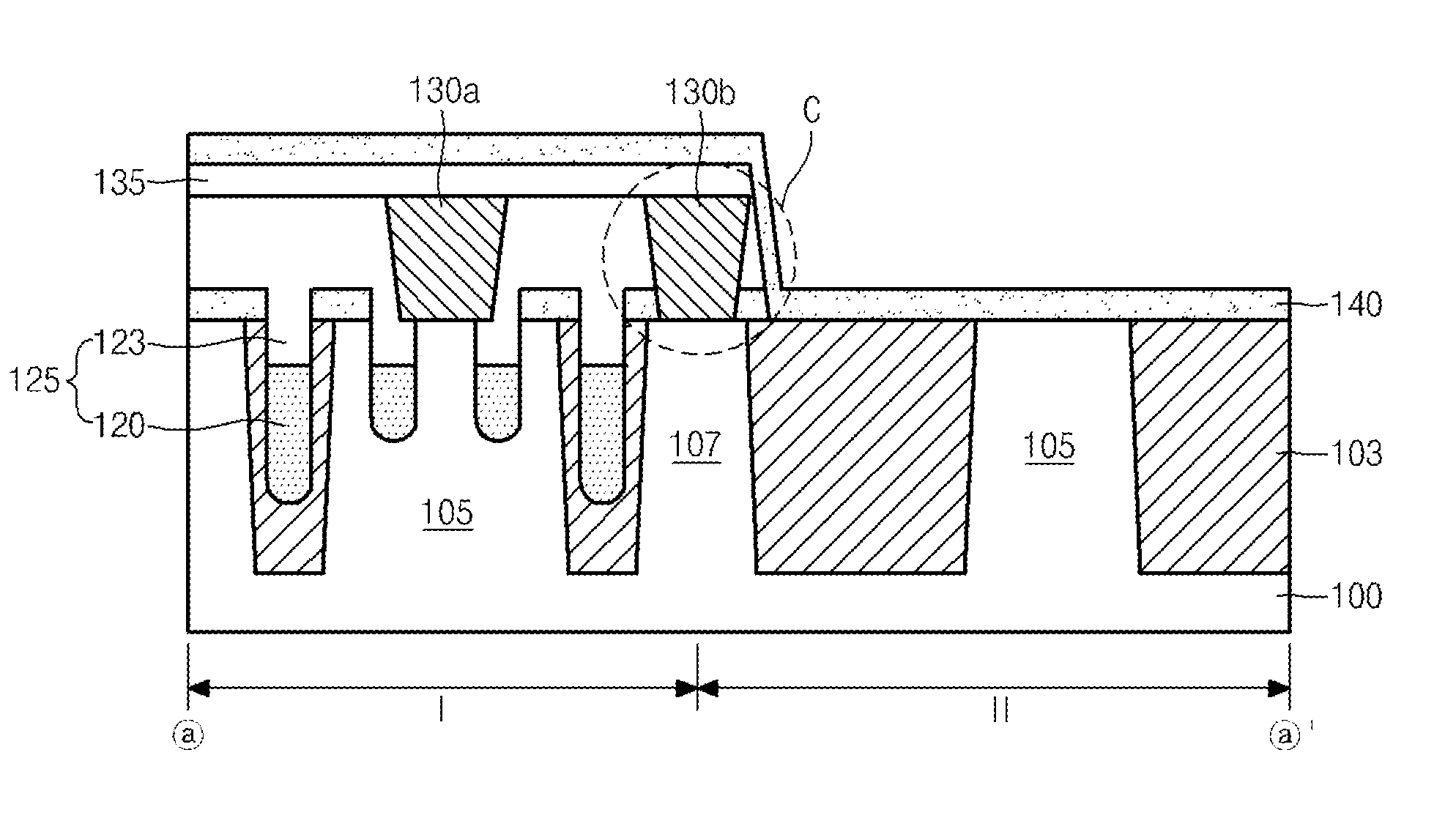
[0028]Referring to FIG. 3, a semiconductor device includes a cell region I and a peripheral region II. In the cell region I, a device isolation structure 103 that defines a first active region 105 is formed, and a plurality of first gates 125a are formed in the first active region 105. The first gate 125a may be a buried-type gate, but is not limited thereto. In the first active region 105, two first gates 125a can be formed. A bit line contact plug 130 is formed on the first active region 105 between the first gates 125a. A bit line (not shown) that contacts the bit line contact plug 130 is formed perpendicular to the first gate 125a.

[0029]A second active region 107 that serves as a guard ring is formed between the cell region I and the peripheral region II. In the se...


PUM


Abstract

A semiconductor device including a cell region and a peripheral region, the semiconductor device comprising: a guard ring region provided between the cell region and the peripheral region, the guard ring region having a barrier structure.

Description

CROSS-REFERENCE TO RELATED APPLICATION[0001]The priority of Korean patent application No. 10-2010-0037524 filed on Apr. 22, 2010, the disclosure of which is hereby incorporated in its entirety by reference, is claimed.BACKGROUND OF THE INVENTION[0002]An embodiment of the present invention relates to a semiconductor device and a method for manufacturing the same.[0003]Recently, as the data storage capacity of semiconductor memory devices has increased and the integration level has also increased, the size of each unit cell has been required to become smaller. As the integration of the semiconductor device becomes higher, a distance between a gate and a bit line connected to a cell transistor becomes closer. As a result, parasitic capacitance increases to a decrease in the operating reliability of the semiconductor device. In order to improve the reliability of the semiconductor device, a buried-type gate structure has been suggested. In the buried-type gate structure, a conductive ma...

Claims


Application Information

Patent Timeline
IPC IPC(8): H01L29/06H01L21/76
CPCH01L21/76229H01L23/585H01L27/0207H01L27/105H01L29/0607H01L2924/0002H01L27/10894H01L2924/00H10B12/09H01L29/4232
Inventor LEE, DONG GEUNKIM
Owner SK HYNIX INC
Why Eureka
Try Eureka