Solid-state imaging device

a solid-state imaging and imaging device technology, applied in the direction of radiological control devices, instruments, television systems, etc., can solve the problems of inaccurate output signals and degrade image quality, and achieve the effects of smooth horizontal transfer, coupling noise, and reduced voltage of horizontal transfer drive signals

Inactive Publication Date: 2011-10-27
PANASONIC CORP
View PDF3 Cites 4 Cited by
  • Summary
  • Abstract
  • Description
  • Claims
  • Application Information

AI Technical Summary

Benefits of technology

The increase in the number of phases for driving the first horizontal transfer unit is accompanied by an increase in the number of rising and falling edges of pulse waveforms of the drive signals. In the structure according an aspect of the present invention, the horizontal transfer drive signals are driven at a 50% duty cycle, so that the noise which is generated by rising and falling of the drive signals for driving the first horizontal transfer unit can be canceled. Thus, the coupling noise which results from coupling of the above noise in the charge detecting unit can be prevented from occurring in the output voltage. Furthermore, the transfer channel of the second horizontal transfer electrodes is implanted with a higher concentration of acceptor impurities than the first horizontal transfer unit, so that the signal charges can be prevented from flowing back to the first horizontal transfer unit and thus horizontally transferred smoothly.
Furthermore, the present invention can not only provide a solid-state imaging device having the above features, but also provide a camera including such a solid-state imaging device with a structure and an effect which are the same as described above.
In the solid-state imaging device according to an aspect of the present invention, the voltage of the horizontal transfer drive signals is decreased, and the coupling noise which is attributed to rising and falling timing of pulses of the drive signals is reduced, which make it possible to generate accurate image signals and reduce the power consumption.

Problems solved by technology

As shown in FIG. 24, especially when the above coupling noise is generated during the reference voltage integration period and the signal voltage integration period, accurate output signals cannot be obtained, which degrades image quality.

Method used


Image

  • Solid-state imaging device
  • Solid-state imaging device
  • Solid-state imaging device

Examples


first embodiment

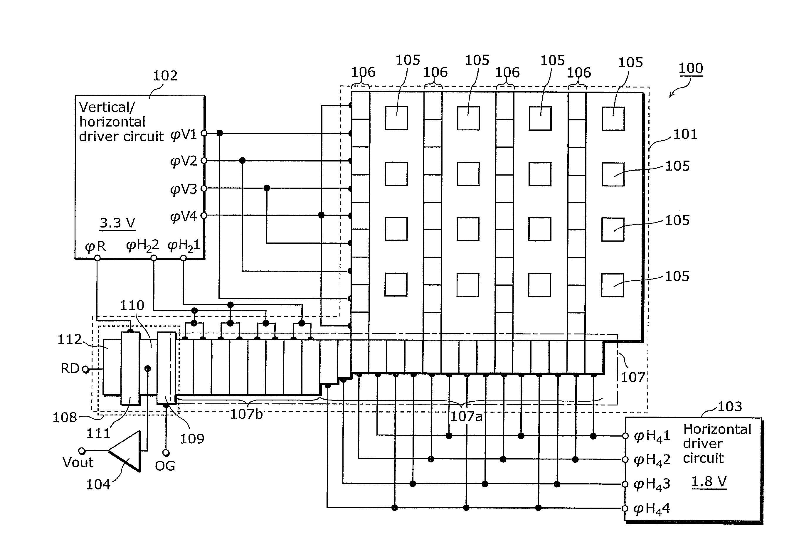
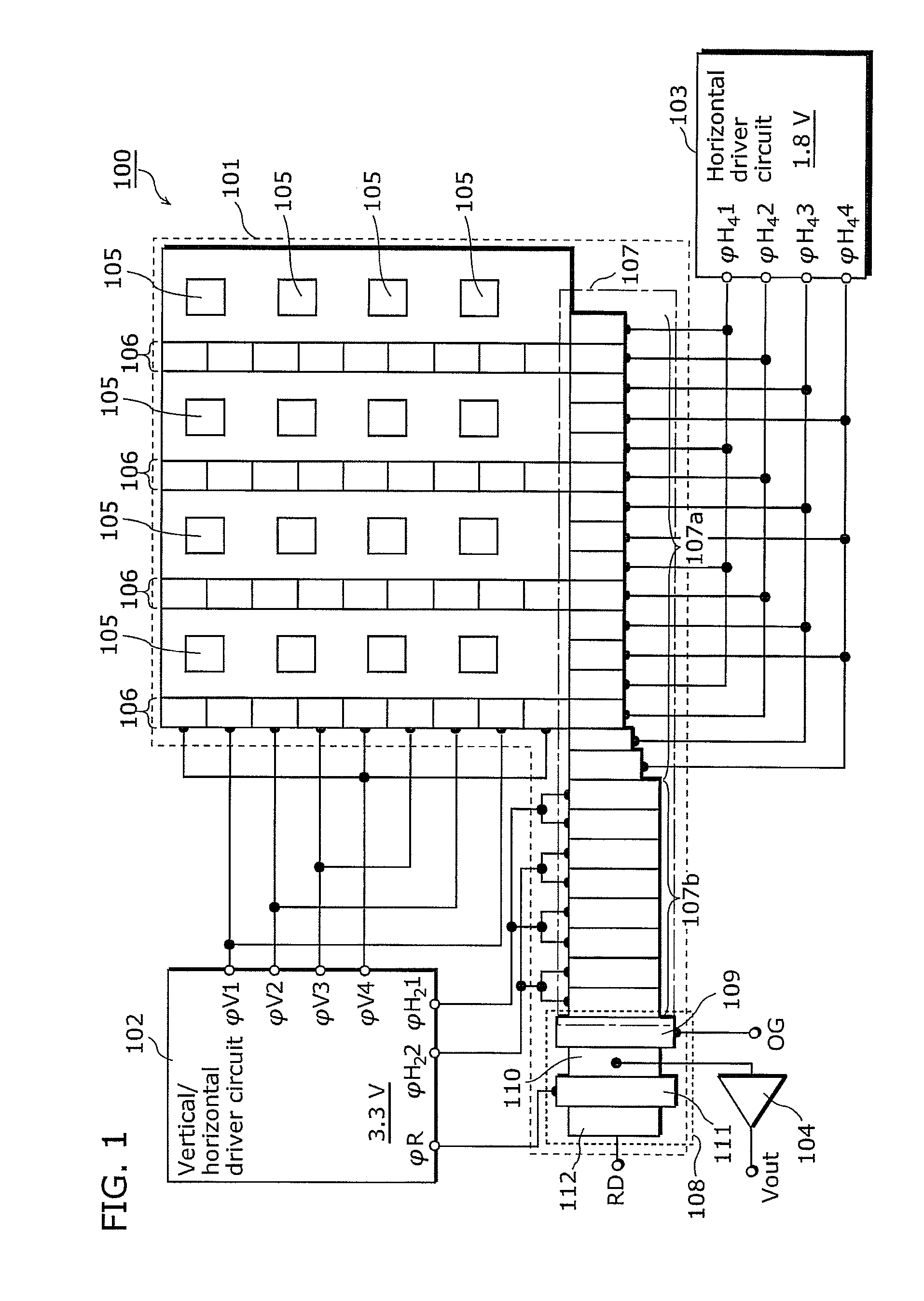
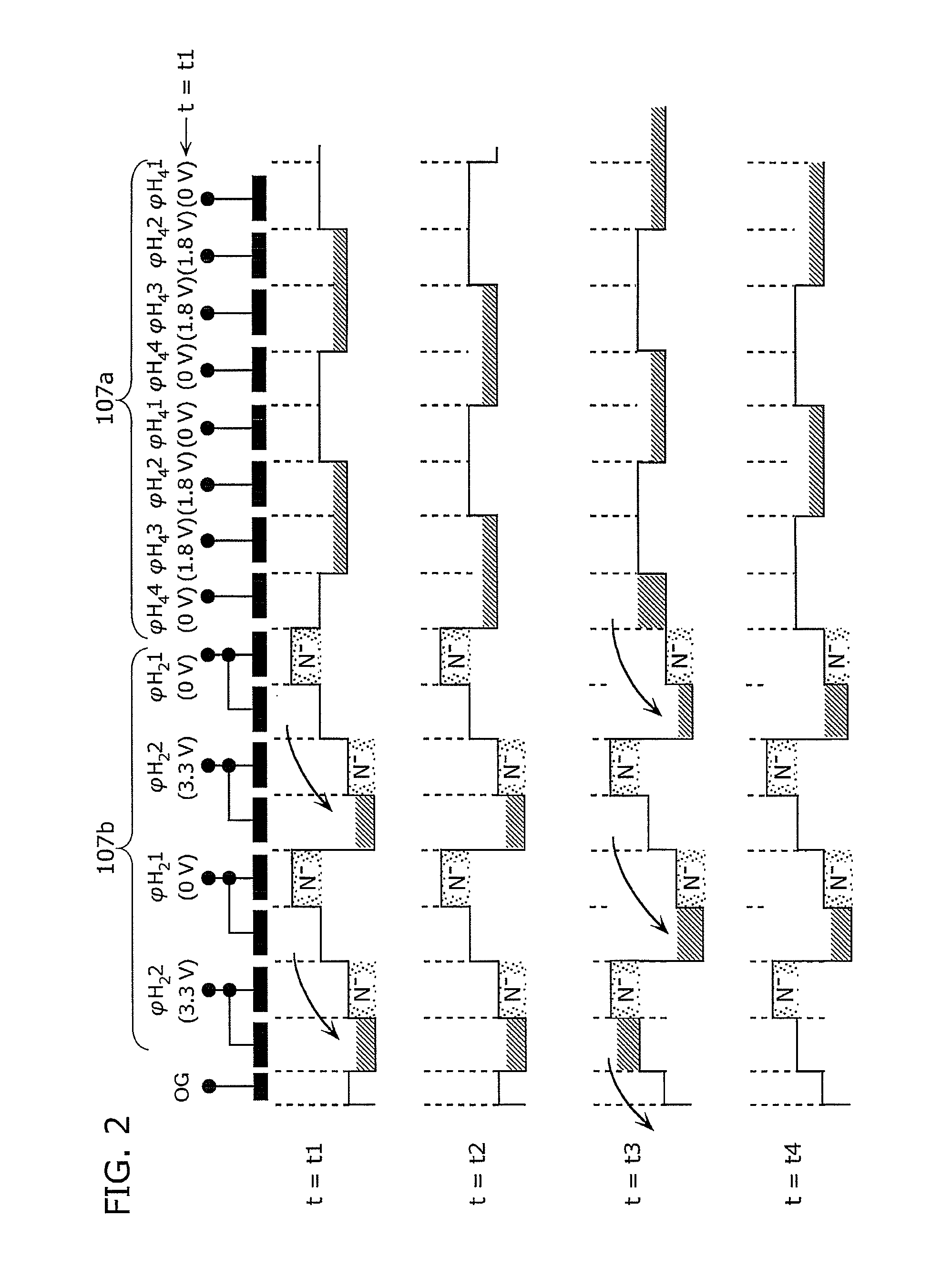
A solid-state imaging device according to the present embodiment includes: a charge detecting unit of a floating diffusion amplifier (FDA) type; a photoelectric conversion element which converts received light into signal charges; a vertical transfer unit configured to vertically transfer the signal charges; a first horizontal transfer unit configured to horizontally transfer the signal charges according to, for example, 4-phase drive signals; and a second horizontal transfer unit spaced apart from the photoelectric conversion element and the vertical transfer unit and disposed between the first horizontal transfer unit and the charge detecting unit, and configured to horizontally transfer the signal charges to the charge detecting unit according to, for example, 2-phase drive signals, the signal charges having been horizontally transferred from the first horizontal transfer unit, wherein a voltage amplitude in each phase of the 4-phse drive signals is smaller than a voltage amplitu...

second embodiment

FIG. 9 illustrates a schematic diagram of a solid-state imaging device according to the second embodiment of the present invention. As shown in FIG. 9, a solid-state imaging device 400 includes the solid-state imaging element 101, a vertical / horizontal driver circuit 402, a horizontal driver circuit 403, and the output amplifier 104. The solid-state imaging element 101 includes: the photoelectric conversion unit made up of the plurality of photoelectric conversion elements 105 arranged in a grid pattern; the plurality of columns of vertical CCD units 106 arranged along the respective columns of the photoelectric conversion elements 105; a horizontal CCD unit 407 disposed on the output terminal side of the respective vertical CCD units 106; and the output unit 108 disposed on the output terminal side of the horizontal CCD unit 407. The solid-state imaging device 400 shown in FIG. 9 is different from the solid-state imaging device 100 according to the first embodiment shown in FIG. 1 ...

third embodiment

FIG. 13 illustrates a schematic diagram of a solid-state imaging device according to the third embodiment of the present invention. As shown in FIG. 13, a solid-state imaging device 500 includes a solid-state imaging element 401, the vertical / horizontal driver circuit 402, a horizontal driver circuit 503, and the output amplifier 104. The solid-state imaging device 500 shown in FIG. 13 is different from the solid-state imaging device 400 according to the second embodiment shown in FIG. 9 in structures and operations of the horizontal driver circuit 503. The following describes only different points from the second embodiment by omitting explanations for the same points.

The horizontal driver circuit 503 serves as the first driver unit which generates 4-phase drive signals φH41, φH42, φH43, and φH44 for driving the front-stage horizontal CCD unit 107a of the horizontal CCD unit 407. Moreover, the horizontal driver circuit 503 serves also as the second driver unit which generates pseud...


PUM


Abstract

A solid-imaging device including an output unit of the FDA type and capable of generating accurate image signals and consuming less power is provided which includes: photoelectric conversion elements; a vertical CCD unit vertically transferring signal charges converted by the photoelectric conversion elements; a front-stage horizontal CCD unit horizontally transferring the signal charges, according to 4-phase drive signals having a 50% duty cycle; a rear-stage horizontal CCD unit disposed between the front-stage horizontal CCD unit and the output unit and horizontally transferring, according to 2-phase drive signals, the signal charges horizontally transferred from the front-stage horizontal CCD unit; a horizontal driver circuit generating the 4-phase drive signals; and a vertical/horizontal driver circuit generating the 2-phase drive signals, wherein the voltage amplitude of the 4-phase drive signals is smaller than the voltage amplitude of the 2-phase drive signals.

Description

BACKGROUND OF THE INVENTION(1) Field of the InventionThe present invention relates to a solid-state imaging device including a charge detecting unit of a floating diffusion amplifier (FDA) type.(2) Description of the Related ArtConventionally, a solid-state imaging device including a charge detecting unit of a floating diffusion amplifier (FDA) type has been known (see Patent Reference 1: Japanese Unexamined Patent Application Publication No. 5-095008).FIG. 18 illustrates a schematic diagram of a conventional solid-state imaging device including a charge detecting unit of the FDA type. As shown in FIG. 18, a solid-state imaging device 700 includes a solid-state imaging element 701, a vertical driver circuit 702, a horizontal driver circuit 703, and an output amplifier 704. The solid-state imaging element 701 includes: a photoelectric conversion element unit made up of a plurality of photoelectric conversion elements 705 arranged in a grid pattern; a plurality of columns of vertical ...

Claims


Application Information

Patent Timeline
Patent Type & Authority Applications(United States)
IPC IPC(8): H04N5/335H01L27/146H01L27/148H04N5/357H04N5/372H04N5/376
CPCH01L27/14812H01L27/14843H04N5/37213H04N5/3577H04N5/335H04N25/00H04N25/617H04N25/713
Inventor NOHARA, TAKUYASUZUKI, SEI
Owner PANASONIC CORP
Why Eureka
Try Eureka