Contactless power transfer system and control method thereof

a power transfer system and control method technology, applied in power conversion systems, ac-dc conversion without reversal, electrical apparatus, etc., can solve the problems of increasing power transfer efficiency, increasing increasing the loss of semiconductor switch, etc., to reduce the number of circuit components, reduce the cost of circuit configuration, and reduce the effect of loss

Active Publication Date: 2012-05-24
FUJI ELECTRIC CO LTD
View PDF4 Cites 54 Cited by
  • Summary
  • Abstract
  • Description
  • Claims
  • Application Information

AI Technical Summary

Benefits of technology

[0034]According to the invention, it is possible to control the direct current output voltage to a constant by a phase control of drive signals of the semiconductor switches configuring the bridge circuit inside the power receiving circuit, without using a constant voltage control circuit as with the heretofore known technology. That is, as the power receiving circuit can be configured of only the bridge circuit and a smoothing capacitor, it is possible to achieve a simplification, miniaturization, and reduction in cost of the circuit configuration. At the same time, it is possible to reduce loss by reducing the number of circuit components, enabling a highly efficient, stable contactless power transfer.

Problems solved by technology

However, for a power converter configuring a high frequency power source device or a power receiving circuit, as the frequency of the current flowing through the circuit increases, the switching loss of the semiconductor switch increases, and the power transfer efficiency decreases, meaning that it is common to set the frequency of the contactlessly fed power between a few kilohertz and a few tens of kilohertz.
1. As the power receiving circuit is configured of the full-wave rectifier circuit 10 and constant voltage control circuit 20, the circuit as a whole increases in size, which leads to an increase in installation space and an increase in cost.
2. As loss also occurs in the reactor L1, semiconductor switch SW1, and diode D1, in addition to in the diodes Du, Dv, Dx, and Dy of the full-wave rectifier circuit 10, these losses cause a decrease in power transfer efficiency.

Method used


Image

  • Contactless power transfer system and control method thereof
  • Contactless power transfer system and control method thereof
  • Contactless power transfer system and control method thereof

Examples


first embodiment

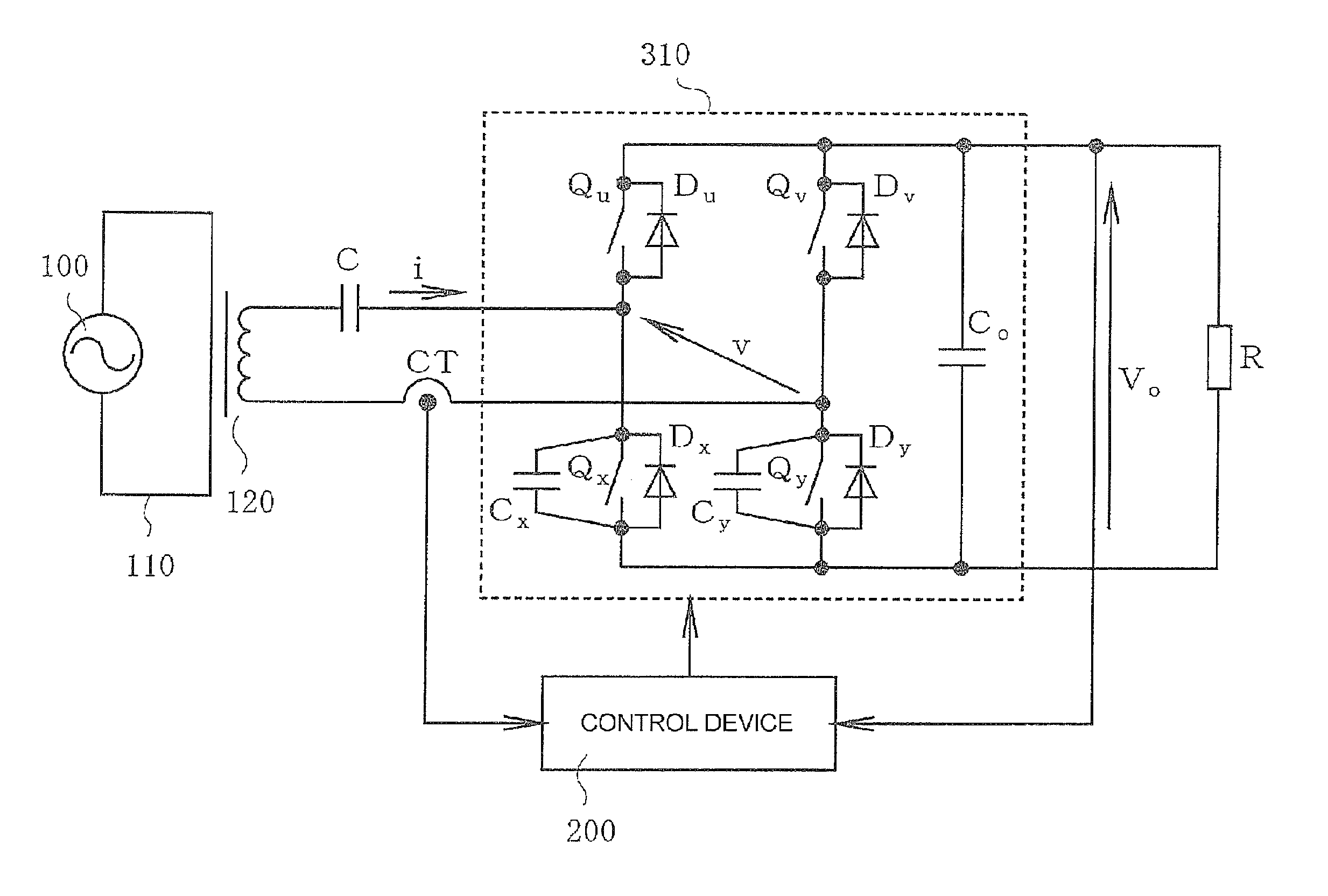
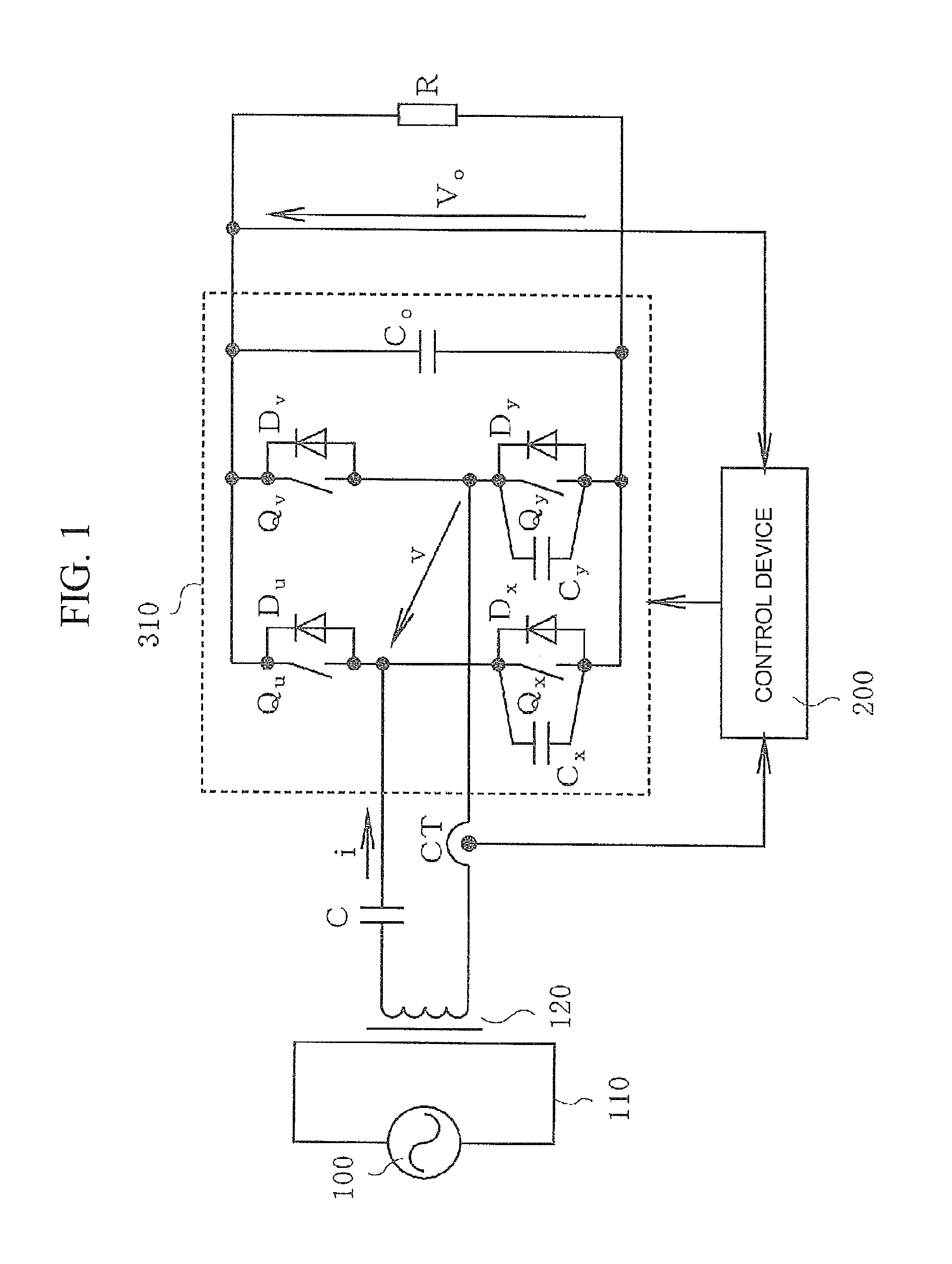
[0063]FIG. 1 is a circuit diagram showing a contactless power transfer system according to the invention, and corresponds to a first aspect of the invention.

[0064]In FIG. 1, reference numeral 310 is a power receiving circuit. The power receiving circuit 310 includes bridge connected semiconductor switches Qu, Qx, Qv, and Qy, diodes Du, Dx, Dv, and Dy connected in reverse parallel to the switches Qu, Qx, Qv, and Qy respectively, capacitors Cx and Cy connected in parallel to the lower arm switches Qx and Qy respectively, and a smoothing capacitor C0 connected between direct current terminals of a bridge circuit (bridge inverter) formed from these elements. A series circuit of a resonant capacitor C and the power receiving coil 120 is connected between alternating current terminals of the bridge circuit, and a load R is connected to either end of the smoothing capacitor C0.

[0065]Also, reference numeral 200 is a control device that generates a drive signal for switching the semiconducto...

second embodiment

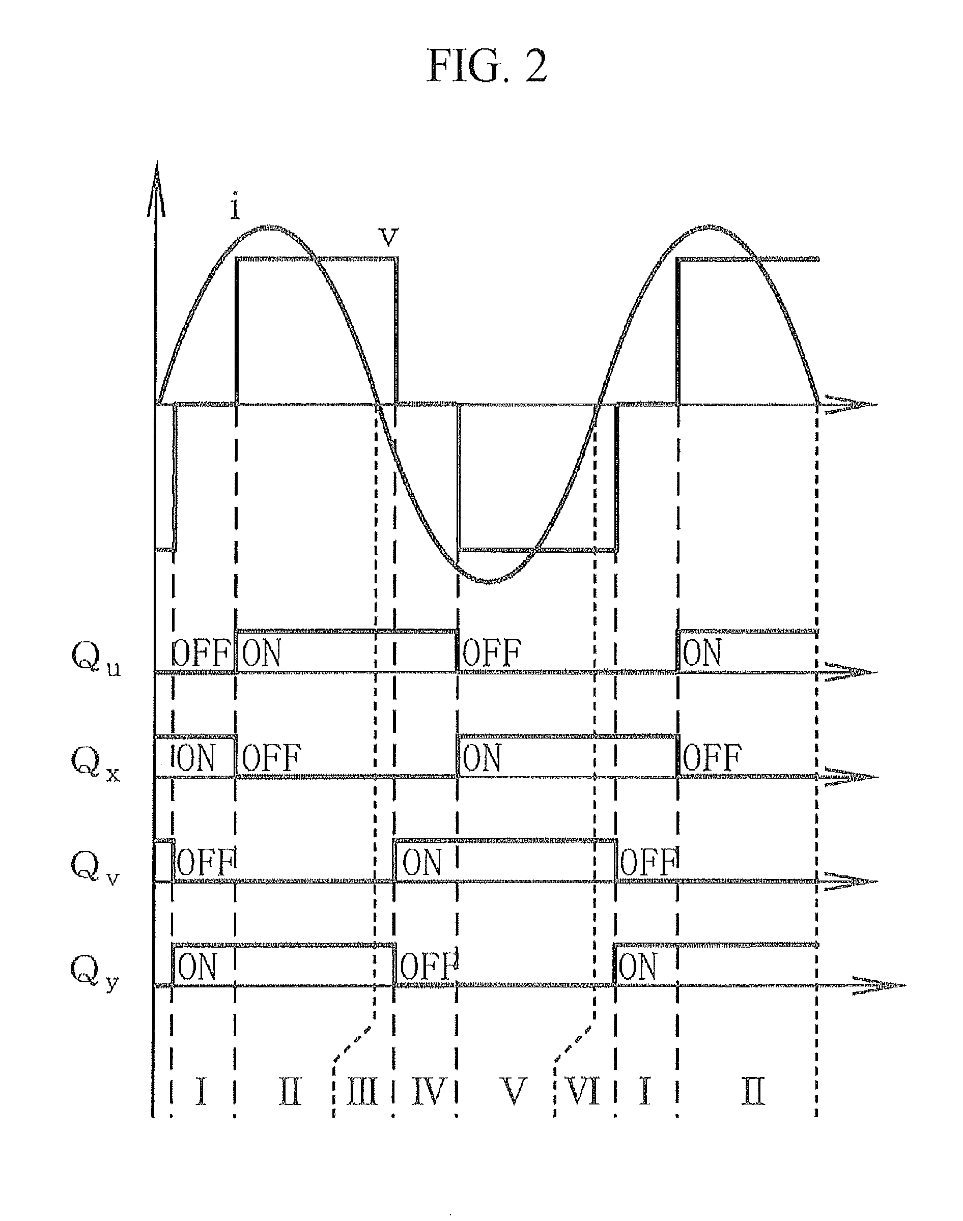
[0102]FIG. 8 is an operation illustration showing the control method according to the invention and, in the same way as FIG. 7, shows an operation waveform of the current i and voltage v, and drive signals of the semiconductor switches Qu, Qx, Qv, and Qy, from a stoppage to a restart of the power transfer from the primary side feeder wire 110.

[0103]When the power transfer is stopped from a normal power transfer condition at a timing (a) of FIG. 8, a loss of the current i is detected by the current detection unit CT in FIG. 1, and the individual semiconductor switches Qu, Qx, Qv, and Qy are controlled into “Qu: off, Qx: on, Qv: off, and Qy: on” conditions.

[0104]This on / off control corresponds to period I shown in FIG. 2, wherein only the lower arm side semiconductor switches Qx and Qy are put into an on condition.

[0105]Next, on the power transfer being restarted at a timing (b) of FIG. 8, a voltage in accordance with a high frequency current of the primary side feeder wire 110 is ind...

third embodiment

[0108]Next, FIG. 9 is an operation illustration showing the control method according to the invention and, in the same way as FIGS. 7 and 8, shows an operation waveform of the current i and voltage v, and drive signals of the semiconductor switches Qu, Qx, Qv, and Qy, from a stoppage to a restart of the power transfer from the primary side feeder wire 110.

[0109]In the embodiment, when the power transfer is stopped from a normal power transfer condition at a timing (a) of FIG. 9, a loss of the current i of the power receiving coil 120 is detected by the current detection unit CT, and the condition of each semiconductor switch Qu, Qx, Qv, and Qy is maintained at the same control condition as immediately before the current i is lost.

[0110]The on / off control of the semiconductor switches Qu, Qx, Qv, and Qy at this time corresponds to period II or period V in FIG. 2. In FIG. 9, as the current i is negative, a case is shown wherein the semiconductor switches Qu, Qx, Qv, and Qy are maintai...


PUM


Abstract

A contactless power transfer system, including a coil configured to supply or receive power contactlessly via magnetic coupling, a bridge circuit having two direct current (DC) terminals and two alternating current (AC) terminals, and a smoothing capacitor connected between the DC terminals. A load is connectable to either end of the smoothing capacitor. One of the AC terminals is connected to one end of the coil via a first capacitor. The other of the AC terminals is connected to the other end of the coil. The bridge circuit includes two serially-connected circuits each having upper and lower arms, each arm having a semiconductor switch and a diode in reverse parallel connection. A second capacitor is connected in parallel to the semiconductor switch of an upper arm, or of a lower arm, or to two semiconductor switches respectively of an upper arm and of a lower arms, of the bridge circuit.

Description

[0001]This application is based on and claims the benefit of priority under 35 U.S.C. §119 from Japanese Patent Application Nos. 2010-257809 and 2011-203097, respectively filed on Nov. 18, 2010 and Sep. 16, 2011, the contents of which are incorporated herein by reference.BACKGROUND OF THE INVENTION[0002]1. Technical Field[0003]The present invention relates to a contactless power transfer system and control method thereof that supply power mainly across a space, utilizing magnetic coupling in a contactless condition between coils.[0004]2. Related Art[0005]A contactless power transfer system supplies power to a load utilizing magnetic coupling between coils caused by electromagnetic induction. The principle thereof is that a sort of transformer is formed by magnetically coupling plural coils across a space, and power is supplied and received utilizing the electromagnetic induction between the coils.[0006]For example, by disposing a primary side coil corresponding to a power supply sou...

Claims


Application Information

Patent Timeline
Patent Type & Authority Applications(United States)
IPC IPC(8): H02M7/06H02M7/12
CPCH02J5/005H02J50/12H02M1/0085
Inventor MARUYAMA, KOUJITOBA, AKIOICHINOSE, AYAKOTAMATE, MICHIO
Owner FUJI ELECTRIC CO LTD
Why Eureka
Try Eureka