With the increasing shrinkage of the features sizes of
semiconductor-based circuit elements such as transistors, thereby significantly increasing the overall complexity of the manufacturing processes, also the complexity of a wiring
system that establishes the
electrical connection of the
semiconductor-based circuit elements and of any other circuit elements has to be adapted to the increasing number of circuit elements and the significantly increased packing density.
For this reason,
copper in combination with so-called low-k
dielectric materials are typically used in complex metallization systems, which, however, may be associated with significant problems in view of the handling of
copper in a semiconductor facility.
Copper, when diffusing into sensitive device areas such as complex
transistor elements, however, may significantly alter the
transistor characteristics and may thus finally result in yield loss and reduced reliability of complex semiconductor devices.
Therefore, complex manufacturing strategies have been developed in forming complex metallization systems in which the
copper material may typically be provided in combination with appropriate conductive and dielectric barrier materials in order to ensure an appropriate copper confinement.
Consequently, upon reducing the dimensions of the circuit elements in the device level, a corresponding
adaptation of the critical dimensions of the contact elements is required, thereby resulting in very complex patterning regimes for forming the contact elements in the interlayer dielectric material.
For a thickness of approximately 1.5 nm and below, however, the corresponding gate leakage currents in sophisticated transistors may reach values that are no longer acceptable for many types of complex semiconductor devices.
Providing a high-k dielectric material in combination with a
metal-containing
electrode material in an early manufacturing stage may result in significant difficulties, for instance for adjusting an appropriate
work function and preserving its value throughout the entire process flow.
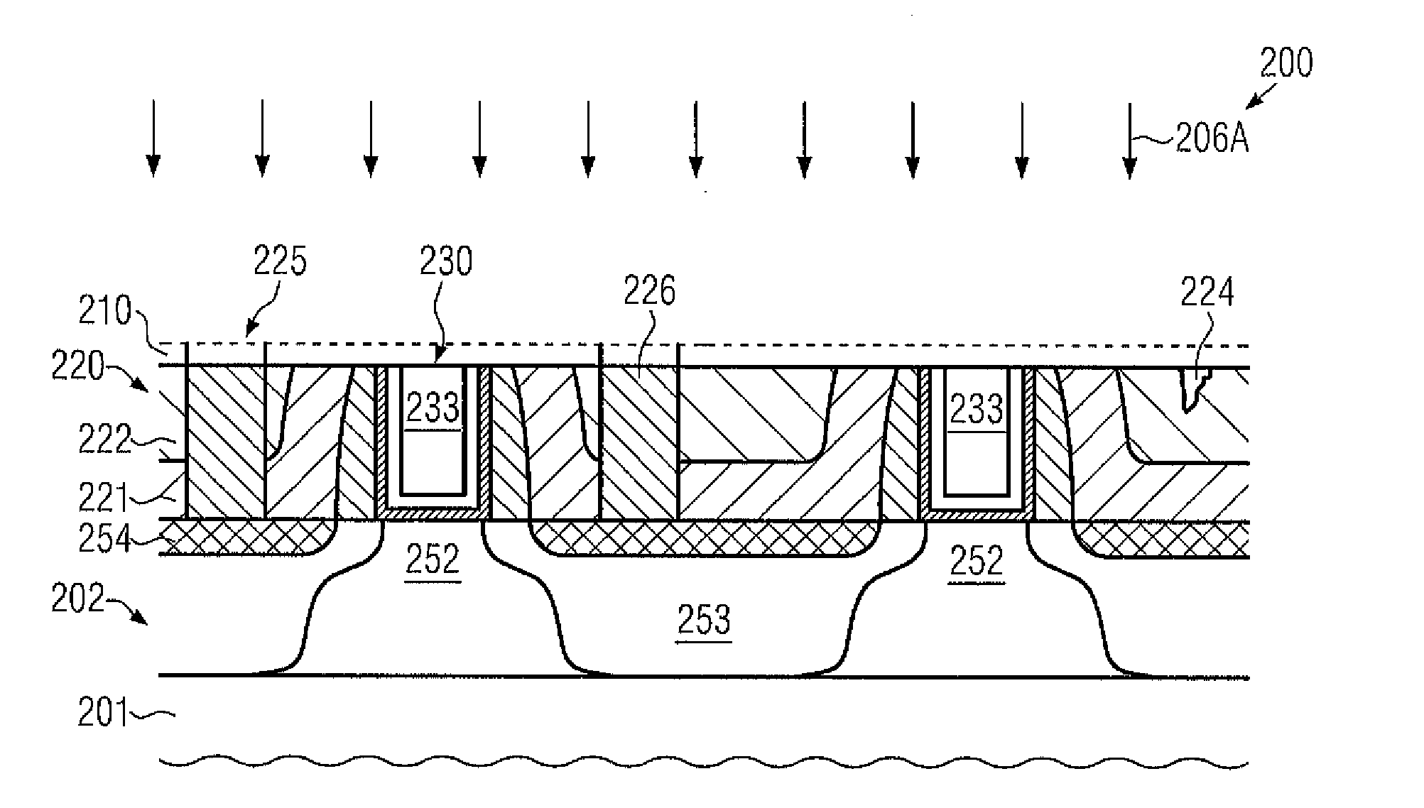
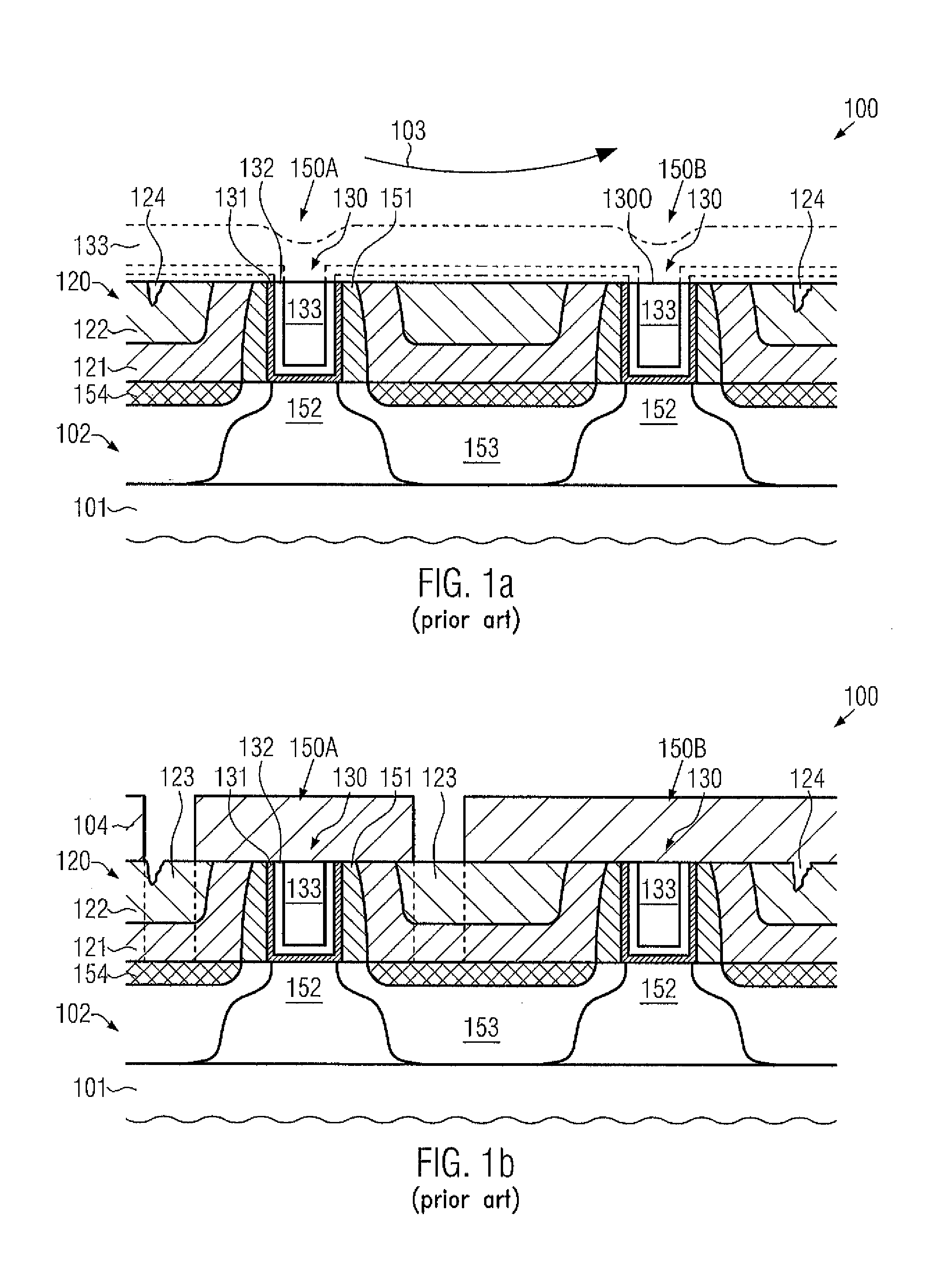
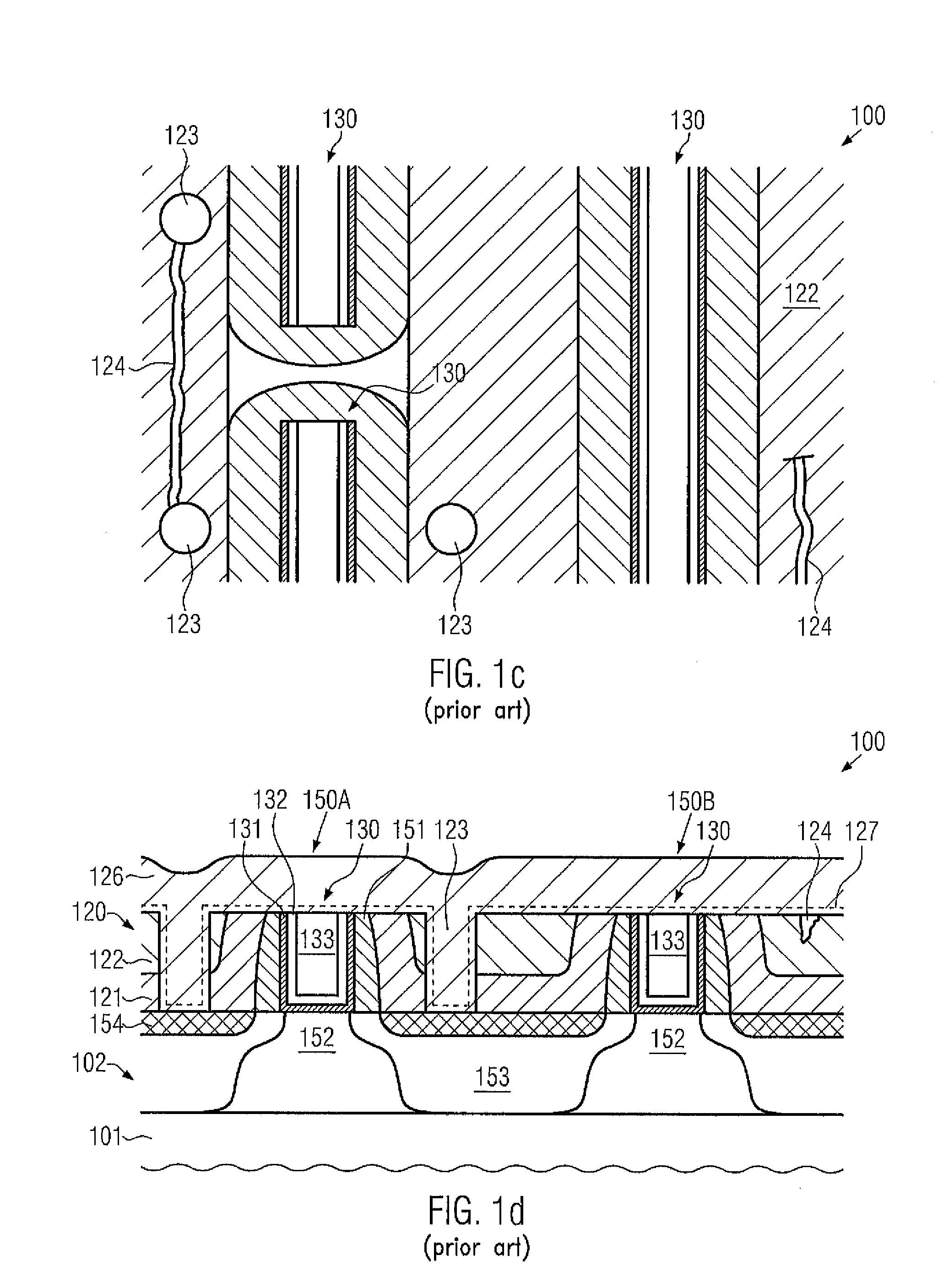
It turns out, however, that in particular the final phase of the replacement gate approach may result in significant defectivity and even device failures upon forming contact elements, as will be explained in more detail with reference to FIGS. 1a-1f.
Furthermore, since a certain over-polish time may have to be applied in order to provide electrically insulated contact elements 125, a corresponding difference in response to the applied
slurry material may thus result in metal depletion, for instance in the contact elements 125.
On the other hand, metal-filled cracks, such as the crack 124 on the left hand side of FIG. 1f, may connect two of the contact elements 125 thereby short-circuiting these contacts 125, which may even result in a total failure of the device 100.
Consequently, in a contact regime using the dielectric material 120 for forming contact elements of
reduced height, the conventional strategy described above may provide significant defectivity and device failures, which may thus contribute to a reduced production yield.
In some conventional approaches, superior
slurry materials may be used during the removal process 105 of FIG. 1e which, however, may require significant research and development efforts for obtaining an appropriate
chemical solution, while nevertheless a desired balance between the chemical response of two different metal materials may nevertheless be very difficult to achieve.
Moreover, the metal-filled cracks may nevertheless contribute to significant contact failures.

