Systems and methods for complementary metal-oxide-semiconductor (CMOS) differential antenna switches using multi-section impedance transformations

a technology of complementary metal oxidesemiconductor and differential antenna switch, which is applied in the field of antenna switches, can solve the problems of linearity degradation of the transmitter and the typical degraded efficiency of the matching network, and achieve the optimal impedance of the differential antenna switch operation, reduce the operating impedance of the switch, and reduce the effect of voltage stress on the receiver switch

Active Publication Date: 2011-11-10
SAMSUNG ELECTRO MECHANICS CO LTD
View PDF5 Cites 46 Cited by
  • Summary
  • Abstract
  • Description
  • Claims
  • Application Information

AI Technical Summary

Benefits of technology

[0006]According to an example embodiment of the invention, there may be an LC balun, which may include plurality of inductors and capacitors. In an example embodiment of the invention, LC balun may combine the output signals of two single-ended antenna switches to transmit the signal through the single-ended antenna, and may provide the optimal impedance for the differential antenna switch operation by impedance transformation. A voltage stress over the receiver switches can be relaxed for a certain level of power with a reduced switch operating impedance which is obtained by implementing the LC balun as an impedance matching network between differential antenna switch and antenna. Thus, the reducing operating impedance of the antenna switch helps to enhance the power handling capability of the antenna switch.
[0007]According to an example embodiment of the invention, there may be a transformer as an output matching network of power amplifiers. To generate a high power, output powers of multiple power amplifiers are combined by an output matching network in transmitter systems. In combining the output powers, transformers are widely used due to its advantage of compact size comparing to the LC counterparts. Since the efficiency of the transformer usually depends on its impedance transformation ratio, the efficiency can be improved by reducing th...

Problems solved by technology

Also, this can cause a device breakdown, which results in linearity degradation of the transmitter.
As...

Method used


Image

  • Systems and methods for complementary metal-oxide-semiconductor (CMOS) differential antenna switches using multi-section impedance transformations
  • Systems and methods for complementary metal-oxide-semiconductor (CMOS) differential antenna switches using multi-section impedance transformations
  • Systems and methods for complementary metal-oxide-semiconductor (CMOS) differential antenna switches using multi-section impedance transformations

Examples


Embodiment Construction

[0017]Example embodiments of the invention now will be described more fully hereinafter with reference to the accompanying drawings, in which some, but not all embodiments of the invention are shown. Indeed, these inventions may be embodied in many different forms and should not be construed as limited to the embodiments set forth herein rather, these embodiments are provided so that this disclosure will satisfy applicable legal requirements. Like numbers refer to like elements throughout.

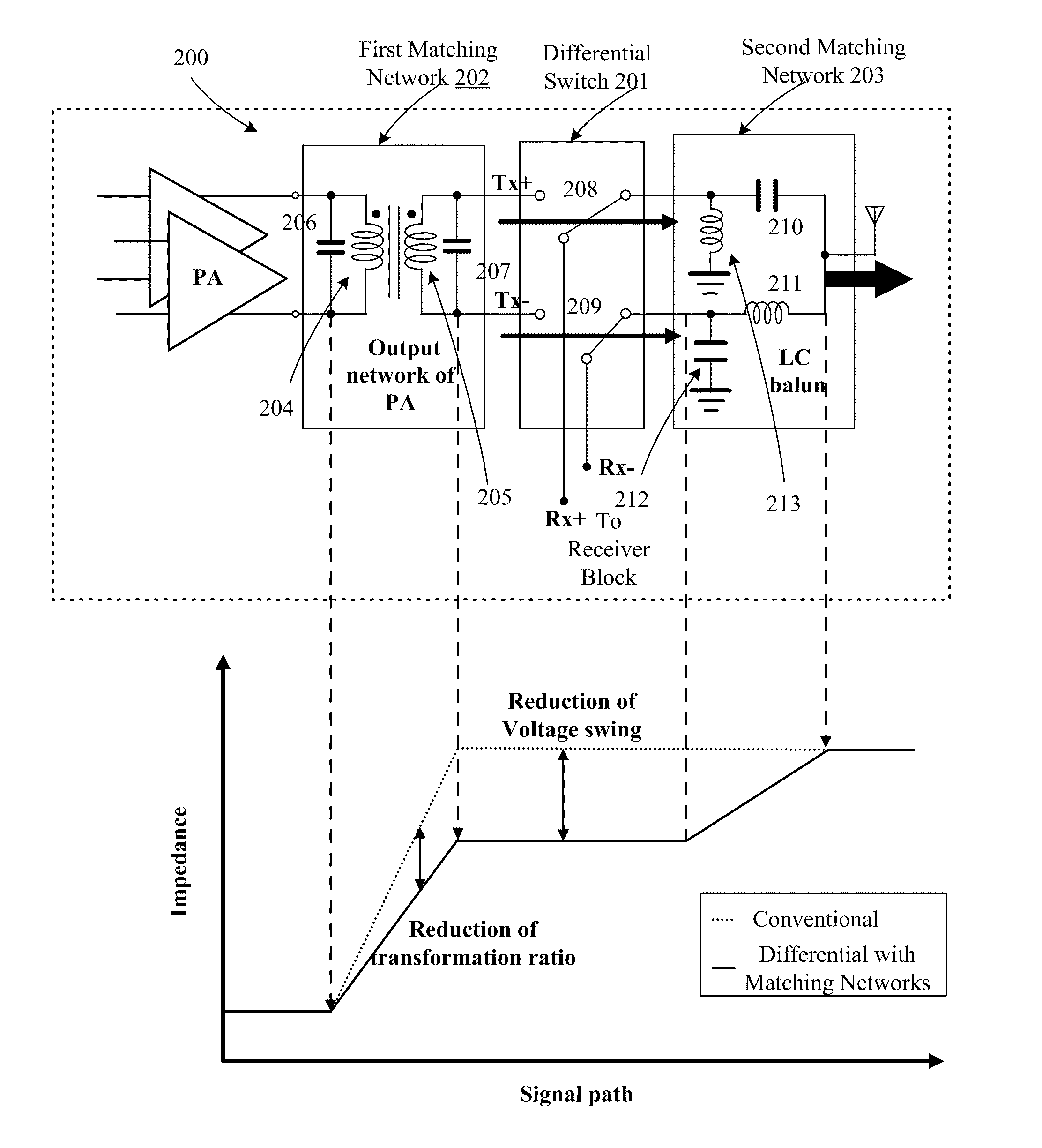
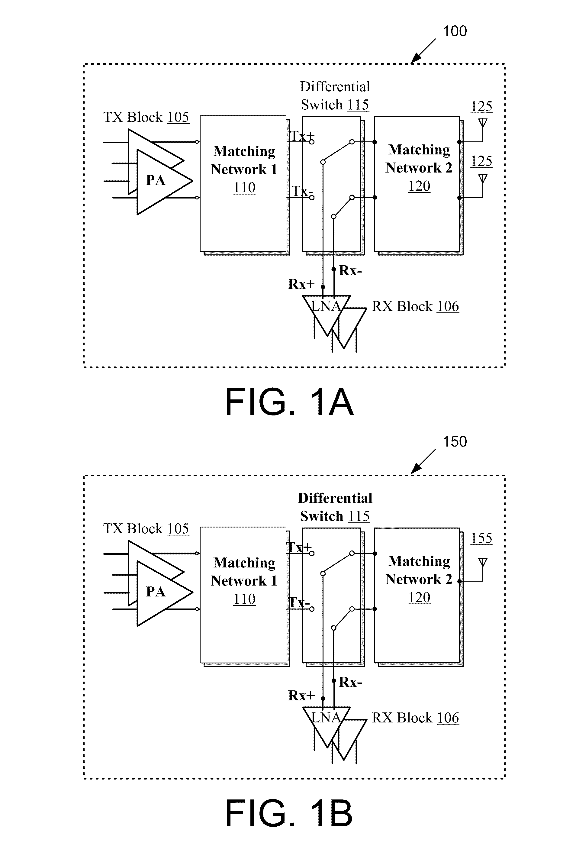
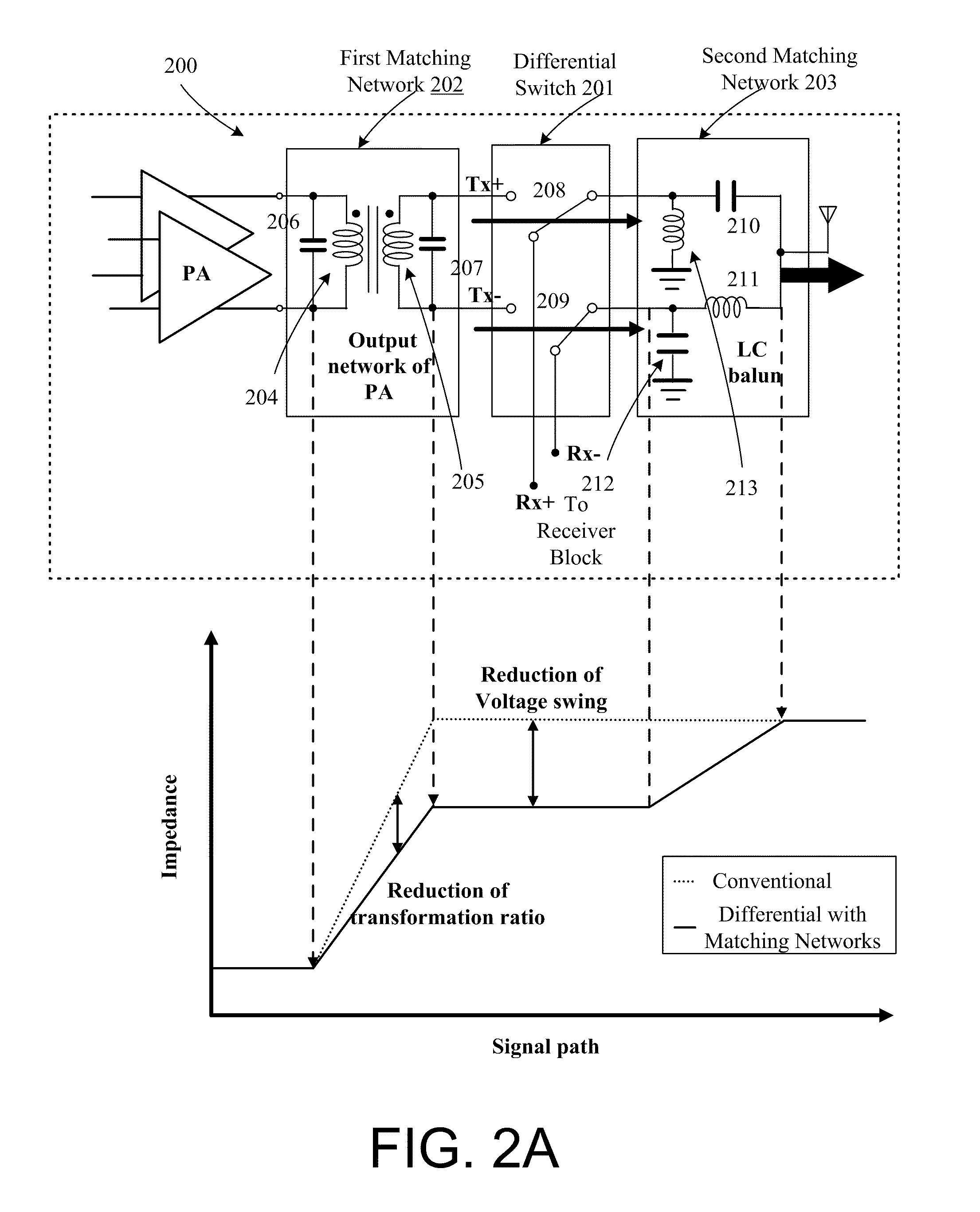
[0018]Example embodiments of the invention may provide for complementary metal-oxide-semiconductor antenna switches. To increase the power handling capability of the CMOS antenna switches, differential switches can be utilized in conjunction with multi-section impedance transformations described herein. Compared to a non-differential structure, differential switches may reduce voltage stress on receiver switches by spreading voltage stress across two or more parallel signal paths. Indeed, the diffe...


PUM


Abstract

Example embodiments of the invention are directed to CMOS differential antenna switches with multi-section impedance transformation. The differential architecture can provide relief from large voltage swings of the power amplifiers by distributing the voltage stress over the receiver switch with two of the identical or substantially similar single-ended switches. In order to reduce the voltage stress further, multi-section impedance transformations can be used. Degraded insertion loss due to the impedance transformation technique can be compensated by selecting an optimal impedance for the antenna switch operation. Accordingly, the use of the multi-section impedance transformations with the differential antenna switch architecture enables high power handling capability for the antenna switch with acceptable efficiency for the transmitter module.

Description

FIELD OF THE INVENTION[0001]The invention relates generally to antenna switches, and more particularly, to systems and methods for complementary metal-oxide-semiconductor (CMOS) differential antenna switches using multi-section impedance transformations.BACKGROUND OF THE INVENTION[0002]In achieving fully integrated wireless communication systems, an antenna switch is utilized to change modes (e.g., transmit and receive modes) or frequency bands (e.g., high and low bands). In performing these tasks, the insertion loss of the antenna switch should be minimized to guarantee a high efficiency of the transmitter as well as a low noise figure of the receiver. The antenna switch should also isolate the receiver from the transmitter effectively during respective receive and transmit modes, and vice versa. In addition, high power signal from the transmitter should be handled without significant distortions by the antenna switch to preserve the linearity of transmitters.[0003]The power handli...

Claims


Application Information

Patent Timeline
IPC IPC(8): H01Q1/50H01Q3/24
CPCH01Q3/24H01Q1/50
Inventor AHN, MINSIKLEE, CHANG-HO
Owner SAMSUNG ELECTRO MECHANICS CO LTD
Why Eureka
Try Eureka