Semiconductor structure, an integrated circuit including a semiconductor structure and a method for manufacturing a semiconductor structure

Active Publication Date: 2011-11-17
NXP USA INC
View PDF2 Cites 28 Cited by
  • Summary
  • Abstract
  • Description
  • Claims
  • Application Information

AI Technical Summary

Benefits of technology

[0001]This invention relates to a semiconductor structure, an integrated circuit including a semiconductor structure and a method for manufacturing a semiconductor structure.
[0007]Specific embodiments of the invention are set forth in the dependent claims. These and other aspects of the invention will be apparent from and elucidated with reference to the embodiments described hereinafter.

Problems solved by technology

III-nitride power semiconductor devices are used for power applications, for example to supply power, due to their high breakdown voltage and low on-resistance.
However, a disadvantage of the known III-nitride power semiconductor devices is that they are discrete devices which need to be connected to other electronic components in order to form an electronic circuit.
Accordingly, the resulting circuit is composed of several dies connected to each other and therefore has a relatively large footprint and is relatively complex to manufacture.
However, such an intrinsic layer is not suited for a Schottky diode, which requires a low current resistance in the forward bias condition.

Method used


Image

  • Semiconductor structure, an integrated circuit including a semiconductor structure and a method for manufacturing a semiconductor structure
  • Semiconductor structure, an integrated circuit including a semiconductor structure and a method for manufacturing a semiconductor structure
  • Semiconductor structure, an integrated circuit including a semiconductor structure and a method for manufacturing a semiconductor structure

Examples


Embodiment Construction

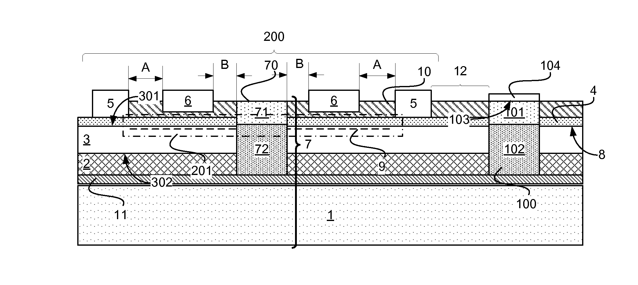
[0013]Referring to FIG. 1 an example of a monolithic semiconductor structure is shown therein. The monolithic semiconductor structure includes a stack of layers. The shown stack of layers comprises a substrate 1, a first layer 3 made from a first semiconductor material and a second layer 4 made from a second semiconductor material. One or more of the first semiconductor material and the second semiconductor material may contain a III-nitride material. The first layer 3 is situated between the substrate 1 and the second layer 4 and more in particular in this example is positioned directly adjacent and in direct contact with the second layer 4 at a second layer side 301 of the first layer 3. Although the first layer 3 may be situated directly adjacent and in direct contact with the substrate 1 at a substrate side 302 of the first layer 3, in the shown example the first layer 3 is separated from the substrate 1 by one or more intermediate layers 2,11.

[0014]The structure includes a powe...


PUM


Abstract

A monolithic semiconductor structure includes a stack of layers. The stack includes a substrate; a first layer made from a first semiconductor material; and a second layer made from a second semiconductor material. The first layer is situated between the substrate and the second layer and at least one of the first semiconductor material and the second semiconductor material contains a III-nitride material. The structure includes a power transistor, including a body formed in the stack of layers; a first power terminal at a side of the first layer facing the second layer; a second power terminal at least partly formed in the substrate; and a gate structure for controlling the propagation through the body of electric signals between the first power terminal and the second power terminal. The structure further includes a vertical Schottky diode, including: an anode; a cathode including the substrate, and a Schottky barrier between the cathode and the anode, the Schottky barrier being situated between the substrate and a anode layer in the stack of layers.

Description

FIELD OF THE INVENTION[0001]This invention relates to a semiconductor structure, an integrated circuit including a semiconductor structure and a method for manufacturing a semiconductor structure.BACKGROUND OF THE INVENTION[0002]III-nitride based power transistors are known in the art. III-nitride power semiconductor devices are used for power applications, for example to supply power, due to their high breakdown voltage and low on-resistance. However, a disadvantage of the known III-nitride power semiconductor devices is that they are discrete devices which need to be connected to other electronic components in order to form an electronic circuit. Accordingly, the resulting circuit is composed of several dies connected to each other and therefore has a relatively large footprint and is relatively complex to manufacture.[0003]United States Patent Application Publication US 2006 / 0175633 discloses a monolithic integrated III-nitride power device which includes a hetero-junction III-ni...

Claims


Application Information

Patent Timeline
IPC IPC(8): H01L29/16H01L29/20H01L21/329H01L29/778
CPCH01L21/746H01L27/0605H01L27/0629H01L29/0847H01L29/2003H01L29/872H01L29/517H01L29/518H01L29/66462H01L29/7787H01L29/4175
Inventor RENAUD, PHILIPPE
Owner NXP USA INC
Why Eureka
Try Eureka