Power core for use in circuitized substrate and method of making same

a power core and circuitized substrate technology, applied in the field of circuitized substrates, can solve the problems of inability to resist stress, device or electrical connection between them, and the non-optimal (excessive) thermal expansion coefficient of the overall pcb and the individual layers, etc., to achieve the effect of improving the circuitized substrate ar

Active Publication Date: 2011-11-24
TTM TECH NORTH AMERICA LLC
View PDF5 Cites 13 Cited by
  • Summary
  • Abstract
  • Description
  • Claims
  • Application Information

AI Technical Summary

Benefits of technology

[0035]It is a primary object of the present invention to enhance the circuitized substrate art, and particularly that part of the art involving power core assemblies.
[0038]It is still another object of the invention to provide such a method which may be accomplished in a relatively facile manner and at relatively low cost in comparison to some known substrate manufacturing processes.

Problems solved by technology

PCBs used today are generally much more complex, however, and are usually made of metal power and ground planes and several signal planes containing circuit lines sandwiched in an alternative manner between several layers of dielectric material, often with metal lines and pads on the top and bottom surface of the multilayered “sandwich.” Top and bottom conductors may be connected with one other as well as with selected internal circuit layers using conductive “thru holes”, e.g., Plated Through Holes (PTHs).
There are still, however, problems associated with these products, many of which are brought on by the aforementioned demands for greater capabilities while offering a smaller scale final product.
One of the causes of some problems is a non-optimal (excessive) coefficient of thermal expansion (CTE) mismatch for the overall PCB and the individual layers.
Many PCBs and LCCs are generally composed largely of organic materials, and thus tend to have a higher CTE that is not well matched to the CTE of the silicon chip or chips positioned thereon.
Sometimes these devices or the electrical connections between them cannot withstand the stress, particularly after repeated temperature cycling.
When solder is used to bond the devices to the substrate (e.g., a chip is connected to the LCC through small solder bumps some of which are called Controlled Collapse Chip Connections (C4) in the art), excessive expansion of the supporting structure may result in damage and even separation of the various solder bonds, thereby rendering the package inoperable for the intended purpose.
This adds of course to the total package cost and is not always completely effective when extremely high temperatures might be encountered or if the CTE mismatch is excessive.
Further, the chip / PCB or LCC CTE mismatch may result in the assembled package warping, putting tensile stress on the chip to the extent that it might crack and thus be destroyed.
Yet another adverse result caused by the CTE differential is shear induced de-bonding, where the dielectric may in fact be torn from the power / ground planes.
Shear induced de-bonding exacerbates the CTE-caused cracking mechanisms because the de-bonded dielectric is essentially “floating” and is not connected to the metallic power / ground planes.

Method used


Image

  • Power core for use in circuitized substrate and method of making same
  • Power core for use in circuitized substrate and method of making same
  • Power core for use in circuitized substrate and method of making same

Examples


Embodiment Construction

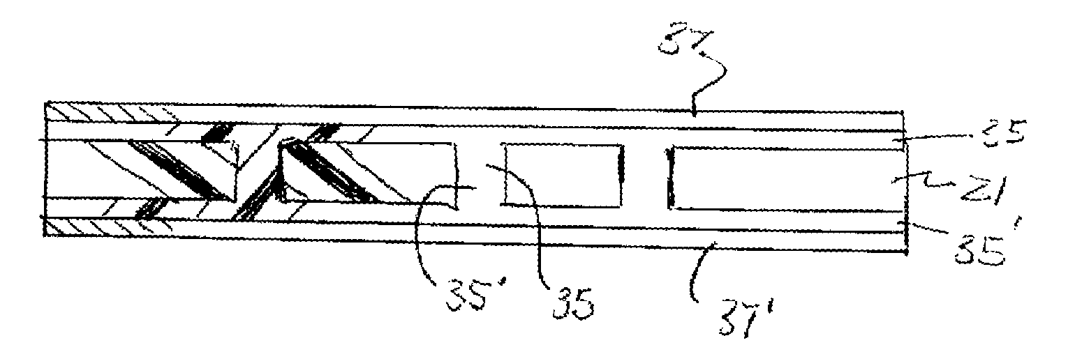
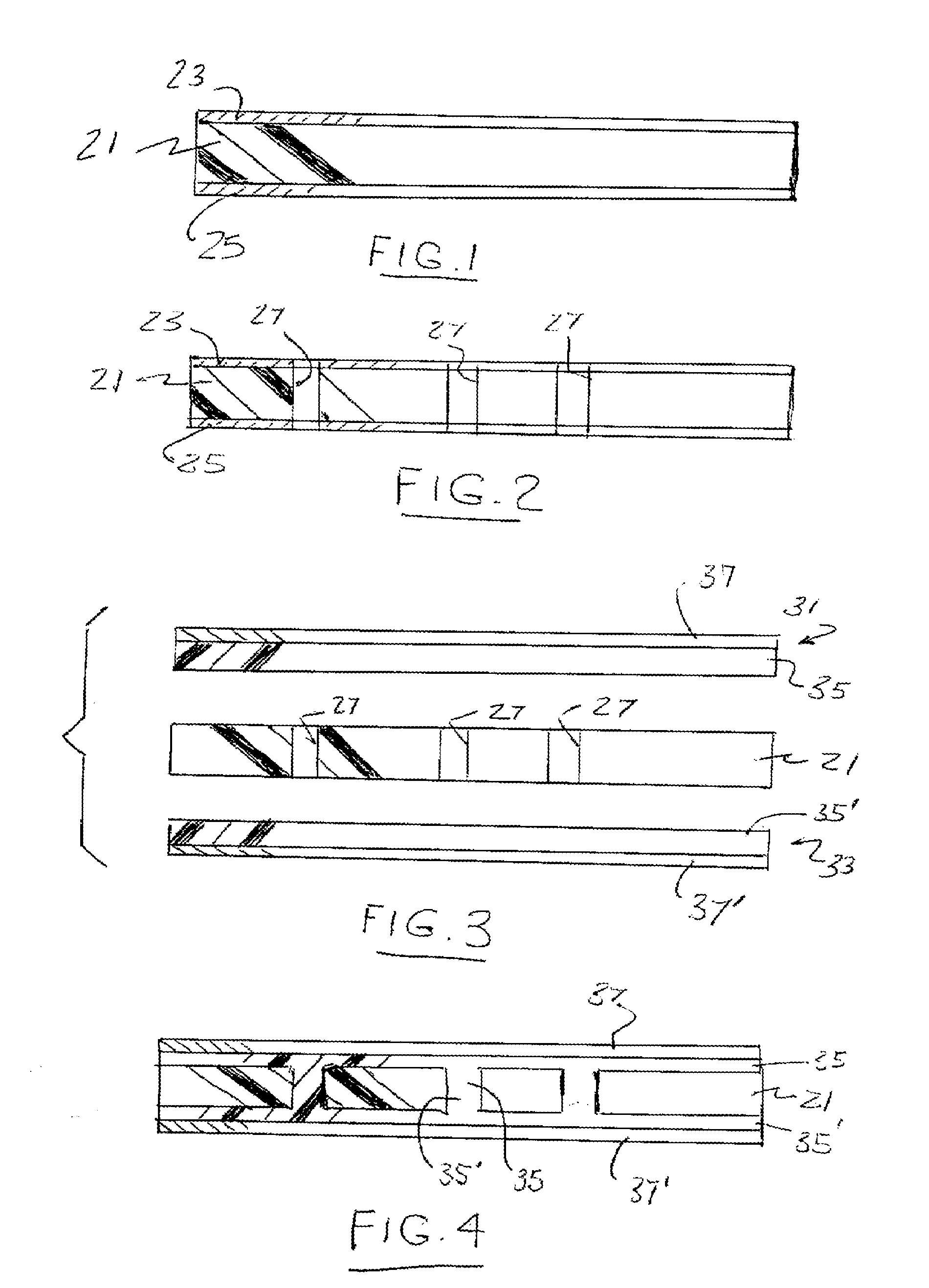
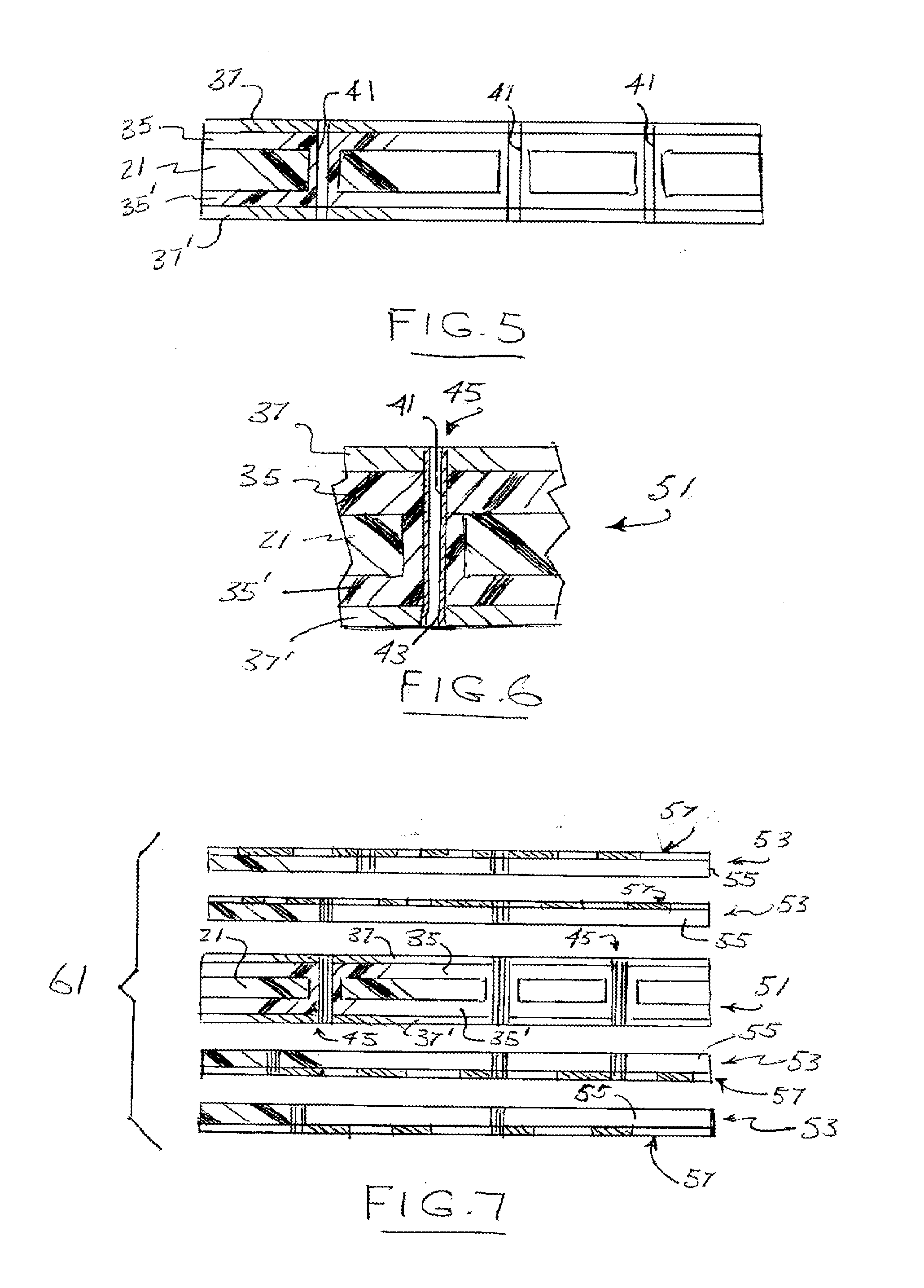
[0048]For a better understanding of the present invention, together with other and further objects, advantages and capabilities thereof, reference is made to the following disclosure and appended claims in connection with the above-described drawings. It is understood that like numerals will be used to indicate like elements from drawing figure to drawing figure.

Definitions

[0049]The following terms will be used herein and are understood to have the meanings associated therewith.

[0050]By the term “circuitized substrate” as used herein is meant to include multilayered structures including a plurality of dielectric layers and a plurality of circuitized conductive layers typically arranged in an alternating manner. Examples of dielectric materials suitable for use in such structures include fiberglass-reinforced or non-reinforced epoxy resins, poly-tetrafluoroethylene (Teflon), polyimides, polyamides, cyanate resins, photoimageable materials, ceramic and other like materials, or combina...


PUM

PropertyMeasurementUnit
sizeaaaaaaaaaa
sizeaaaaaaaaaa
dielectric constantaaaaaaaaaa

Abstract

A power core adapted for use as part of a circuitized substrate, e.g., a PCB or LCC. The core includes a first layer of low expansion dielectric and two added layers of a different low expansion dielectric bonded thereto, with two conductive layers positioned on the two added low expansion dielectric layers. At least one of the conductive layers serves as a power plane for the power core, which in turn is usable within a circuitized substrate, also provided. Methods of making the power core and circuitized substrate are also provided. The use of different low expansion dielectric materials for the power core enables the use of support enhancing fiberglass in one layer while such use is precluded in the other two dielectric layers, thus preventing CAF shorting problems in highly precisely defined thru holes formed within the power core.

Description

FIELD OF THE INVENTION[0001]The present invention relates to circuitized substrates, e.g., Printed Circuit Boards (PCBs), Laminated Chip Carriers (LCCs) and the like, and more particularly to power cores for use in such substrates. The present invention also relates to methods for fabricating such structures.BACKGROUND OF THE INVENTION[0002]Information handling systems such as computers and similar electronic equipment have become essential in the lives of many people today. Many businesses, banks, and governments rely on such systems, particularly computers, as part of their everyday activities. Because of the relatively complex demands placed on these systems, it is essential that said systems be highly reliable and stable. Computers today, for example, are required to run longer, operate at higher frequencies (signal speeds) and exhibit less downtime than at any time in the past. Accordingly, if each component utilized in such systems is designed to last longer and be more reliab...

Claims


Application Information

Patent Timeline
Patent Type & Authority Applications(United States)
IPC IPC(8): H05K1/09H05K1/00H01R43/00H05K1/11
CPCH05K3/4617Y10T29/49117H05K2201/068H05K3/4641
Inventor JAPP, ROBERT M.PAPATHOMAS, KOSTASKRESGE, JOHN S.ANTESBERGER, TIMOTHY
Owner TTM TECH NORTH AMERICA LLC
Why Eureka
Try Eureka