Semiconductor device and method of manufacturing semiconductor device

a semiconductor device and semiconductor technology, applied in the direction of semiconductor devices, semiconductor/solid-state device details, capacitors, etc., can solve the problems of excessive etching, degraded yield of semiconductor devices, and difficulty in filling up such high-aspect-ratio trenches with electrodes which compose capacitor elements, etc., to achieve excellent yield, good yield, and excessive etching or insufficient etching

Active Publication Date: 2011-11-24
RENESAS ELECTRONICS CORP
View PDF2 Cites 32 Cited by
  • Summary
  • Abstract
  • Description
  • Claims
  • Application Information

AI Technical Summary

Benefits of technology

[0049]In the present invention, the top surface of the upper interconnect, and the top surface of the interconnect configuring the logic circuit are aligned to the same plane. Accordingly, excessive etching or insufficient etching may be suppressed above the top surface of the upper interconnect. The upper interconnect and the embedded electrode herein are configured by the same material in an integrated manner. It is therefore no longer necessary, in the process of forming the upper interconnect, to etch the embedded electrode by the etch-back process in order to ensure a space for forming the upper interconnect. Accordingly, the embedded electrode may be suppressed from being excessively etched.
[0050]As may be understood from the above, the present invention has a structure excellent in the yield.
[0051]According to the present invention, a semiconductor device having a structure manufacturable in good yield, and a method of manufacturing the same are provided.

Problems solved by technology

For this reason, it has been very difficult to fill up such high-aspect-ratio trenches with the electrode which composes the capacitor elements.
The etch-back process has, however, occasionally resulted in an excessive removal of the top surface of the capacitor elements 301, and has consequently degraded yield of the semiconductor device.
This has resulted, for example, in excessive etching of the upper interconnects of the capacitor elements in the process of forming connecting portions towards the upper interconnects, or has conversely resulted in insufficient etching of the insulating film in the process of forming the connecting portions towards the upper interconnects.
As a consequence, the techniques described in Japanese Laid-Open Patent Publication Nos. 2000-332216, 2004-342787 and 2005-101647 have occasionally been suffering from degradation in yield of the semiconductor devices.

Method used


Image

  • Semiconductor device and method of manufacturing semiconductor device
  • Semiconductor device and method of manufacturing semiconductor device
  • Semiconductor device and method of manufacturing semiconductor device

Examples


first embodiment

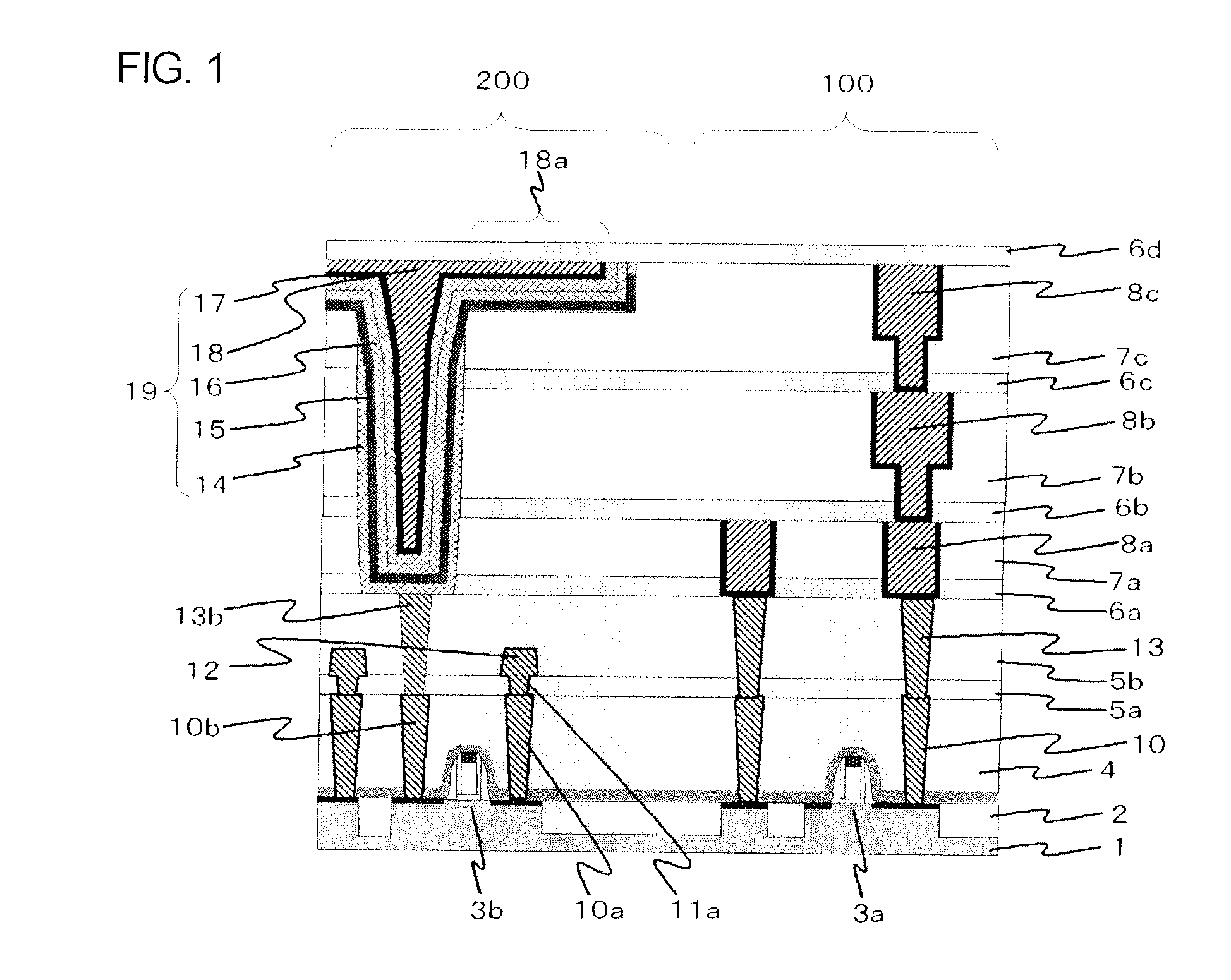
[0073]A semiconductor device of a first embodiment will be explained.

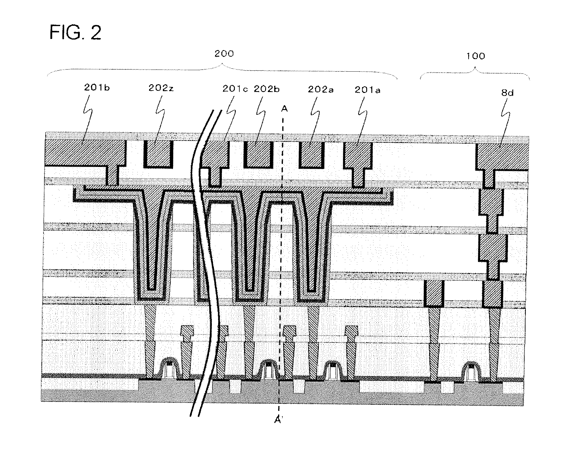
[0074]FIG. 1 and FIG. 2 are sectional views schematically illustrating a semiconductor device of a first embodiment. FIG. 1 is an extraction of a portion on the right side, as seen in the drawing, of dashed line A-A′ in FIG. 2 for simplicity. FIG. 9 is a top view schematically illustrating the semiconductor device of the first embodiment.

[0075]The semiconductor device of this embodiment has a substrate (semiconductor substrate 1); a multi-layered interconnect formed on the semiconductor substrate 1, and having a plurality of interconnect layers, each of which being configured by an interconnect and an insulating layer, stacked therein; a memory circuit 200 formed in a memory circuit region on the semiconductor substrate 1 in a plan view, and having a peripheral circuit and at least one capacitor element 19 embedded in the multi-layered interconnect; and a logic circuit 100 formed in a logic circuit region on the se...

second embodiment

[0161]Next, a semiconductor device of a second embodiment will be detailed, referring to the attached drawings.

[0162]FIG. 4 is a sectional view illustrating the second embodiment. Unlike the first embodiment of the present invention previously illustrated in FIG. 1, the semiconductor device of the second embodiment has, as illustrated in FIG. 4, a vertical interconnect 203 formed below the extension electrode 18a of the upper interconnect 18 of the capacitor element 19, so as to extend through the upper electrode 16 and the capacitor insulating film 15 towards the substrate. Through the vertical interconnect 203, the extension electrode 18a of the upper interconnect 18 of the capacitor element 19, and the fixed-potential interconnect 201 positioned below the extension electrode 18a are connected. The vertical interconnect 203 may be formed for each of, or a part of the plurality of capacitor elements 19. The upper interconnect 18 and the vertical interconnect 203 are configured by t...

third embodiment

[0174]Next, a semiconductor device of a third embodiment will be explained referring to the attached drawings.

[0175]FIG. 6 is a sectional view illustrating the semiconductor device of the third embodiment. In the third embodiment, unlike the first embodiment and the second embodiment, the top surface of the upper interconnect 18 of the capacitor element 19 is formed so as to be aligned to the same plane with the top surface of the interconnect 8b of the logic circuit. More specifically, the height in the thickness-wise direction of the capacitor element 19 is equivalent to the multi-layered interconnect composed of two interconnect layers, which is smaller than those in the first and second embodiments. By virtue of this configuration, a larger number of interconnects in the memory circuit is now adoptable to applications other than the capacitor element, and the circuit design may therefore be simplified. While electrostatic capacity of the capacitor element 19 inevitably decreases...


PUM


Abstract

A semiconductor device has a substrate; a multi-layered interconnect formed on the substrate, and having a plurality of interconnect layers, each of which being configured by an interconnect and an insulating layer, stacked therein; a memory circuit formed in a memory circuit region on the substrate in a plan view, and having a peripheral circuit and at least one capacitor element embedded in the multi-layered interconnect; and a logic circuit formed in a logic circuit region on the substrate, wherein the capacitor element is configured by a lower electrode, a capacitor insulating film, an upper electrode, an embedded electrode and an upper interconnect; the top surface of the upper interconnect, and the top surface of the interconnect configuring the logic circuit formed in the same interconnect layer with the upper interconnect, are aligned to the same plane.

Description

[0001]This application is based on Japanese patent application No. 2010-115755 and No. 2010-270310 the content of which is incorporated hereinto by reference.BACKGROUND[0002]1. Technical Field[0003]The present invention relates to a semiconductor device and a method of manufacturing a semiconductor device.[0004]2. Related Art[0005]Advancement of performance of semiconductor devices has been driven mainly by shrinkage of element. One of effects ascribable to the shrinkage relates to increase in operational speed of active element, by virtue of shortened gate length. Another effect relates to decrease in occupied area of the semiconductor devices, as a result of shortened gate length and reduced interconnect pitch. As one example making use of increased degree of integration of the semiconductor devices, those having a memory circuit and a logic circuit, which had respectively been formed on separate semiconductor substrates, mounted together on the same semiconductor substrate have a...

Claims


Application Information

Patent Timeline
Patent Type & Authority Applications(United States)
IPC IPC(8): H01L29/92H01L21/02
CPCH01L21/76811H01L23/5223H01L27/10852H01L27/10894H01L28/75H01L2924/0002H01L28/91H01L2924/00H10B12/09H10B12/033H10B99/00H10B12/00
Inventor HIJIOKA, KENICHIROKUME, IPPEIINOUE, NAOYASHIRAI, HIROKIKAWAHARA, JUNHAYASHI, YOSHIHIRO
Owner RENESAS ELECTRONICS CORP
Why Eureka
Try Eureka