Light-emitting device and electronic apparatus

a technology of light-emitting devices and electronic devices, which is applied in the direction of static indicating devices, semiconductor/solid-state device details, instruments, etc., can solve the problems of increasing manufacturing costs, insufficient reduction complicated manufacturing process, etc., and achieves simplified manufacturing process, reduced manufacturing costs, and suppression of resistance of power supply lines

Active Publication Date: 2010-12-21
SEIKO EPSON CORP
View PDF12 Cites 14 Cited by
  • Summary
  • Abstract
  • Description
  • Claims
  • Application Information

AI Technical Summary

Benefits of technology

[0008]An advantage of the invention is that it provides a light-emitting device and an electronic apparatus in which connecting portions and electrical continuity portions are formed from the same layer as that of power supply lines while suppressing the resistance of the power supply lines.
[0009]According to an aspect of the invention, there is provided a light-emitting device including a drive transistor that controls a current to be supplied to a light-emitting element from a power supply line, an electrical continuity portion that electrically connects the drive transistor with the light-emitting element, an initializing transistor that is turned ON to diode-connect the drive transistor, and a connecting portion that electrically connects the drive transistor with the initializing transistor. The power supply line includes a first portion extending in a predetermined direction, and the electrical continuity portion and the connecting portion are formed from the same layer as that of the power supply line and are located on one side along the width of the first portion across the drive transistor. A specific example of this aspect is discussed below as a first embodiment.
[0010]According to this configuration, the electrical continuity portion and the connecting portion are formed from the same layer as that of the power supply line. Thus, the manufacturing process can be simplified and the manufacturing cost can be reduced compared with the configuration in which the electrical continuity portion and the connecting portion are formed from a layer different from that of the power supply line. Additionally, since the electrical continuity portion and the connecting portion are disposed on one side along the width of the first portion across the drive transistor, the space for the power supply line can be ensured on the other side along the width of the first portion across the drive transistor. Thus, a sufficient area (or line width) of the power supply line can be formed so that the resistance of the power supply line can be reduced.
[0011]Forming a plurality of components “from the same layer” is to form the plurality of components in the same step by selectively removing a common film member (it does not matter whether the common film member is a single layer or a plurality of layers), and it does not matter whether the components are connected to each other or are separated from each other.
[0012]It is preferable that the light-emitting device may further include a capacitor element electrically connected to the gate electrode of the drive transistor. In this case, the capacitor element may be disposed opposite the connecting portion and the electrical continuity portion across the drive transistor, and the first portion of the power supply line may be overlapped with the capacitor element. With this arrangement, since the power supply line can be formed such that it is overlapped with the capacitor element, a more sufficient area can be ensured for the power supply line.
[0013]It is preferable that the light-emitting device may further include a selection transistor that is turned ON or OFF according to a selection signal. In this case, the gate electrode of the drive transistor may be set to be a potential corresponding to a data signal supplied from a data line via the selection transistor that is turned ON, and the selection transistor may be disposed opposite the drive transistor across the capacitor element. With this arrangement, a sufficient area (line width) of the power supply line can be ensured, and the configuration of the power supply line can be simplified (for example, without notches) compared with the configuration in which the selection transistor is disposed in the gap between the drive transistor and the capacitor element.

Problems solved by technology

However, if such wiring patterns are formed in different processing steps, the manufacturing process becomes complicated and the manufacturing cost is increased.
Because of such a restriction, for example, a sufficient width of the power supply lines cannot be ensured, and as a result, the resistance of the power supply lines cannot be sufficiently reduced.

Method used


Image

  • Light-emitting device and electronic apparatus
  • Light-emitting device and electronic apparatus
  • Light-emitting device and electronic apparatus

Examples


first embodiment

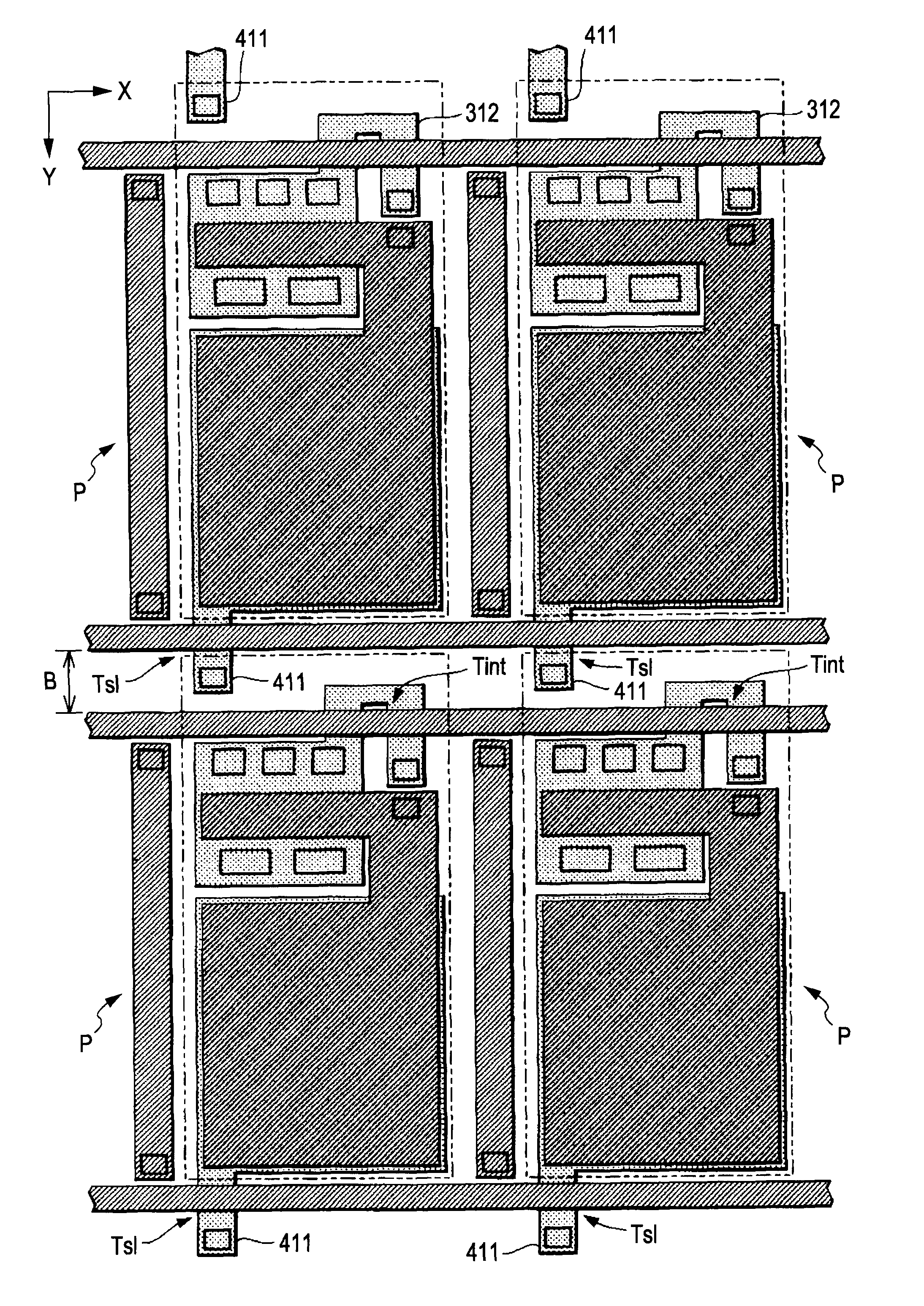
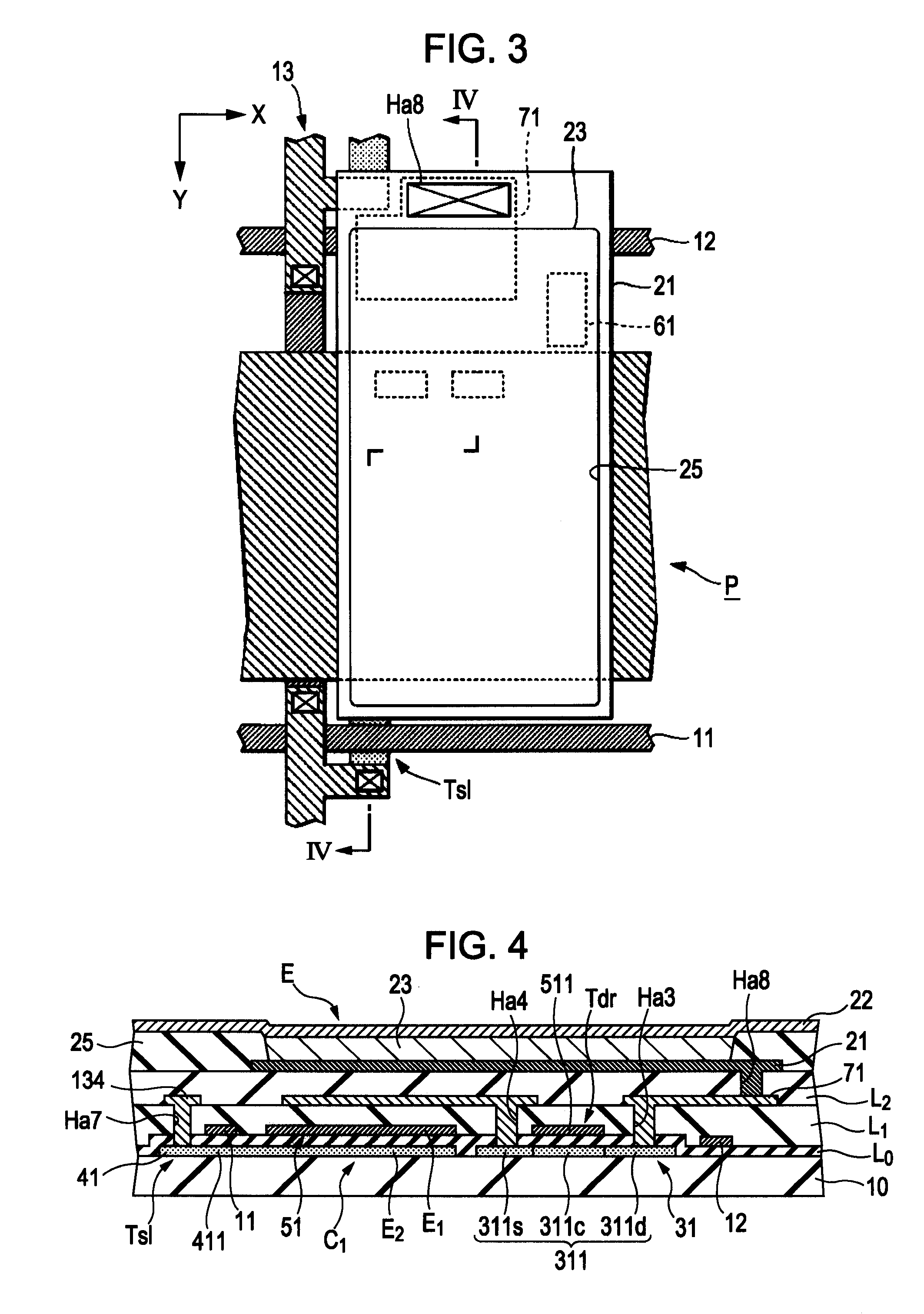
[0062]A description is given below of the specific structure of the unit elements P of the light-emitting device D according to a first embodiment of the invention. FIG. 3 is a plan view illustrating one unit element P, and FIG. 4 is a sectional view taken along line IV-IV of FIG. 3. Although FIG. 3 is a plan view, for easy understanding, the components shown in FIG. 3 corresponding to the counterparts in FIG. 4 are hatched in a manner similar to the counterparts in FIG. 4. The same applies to the other plan views.

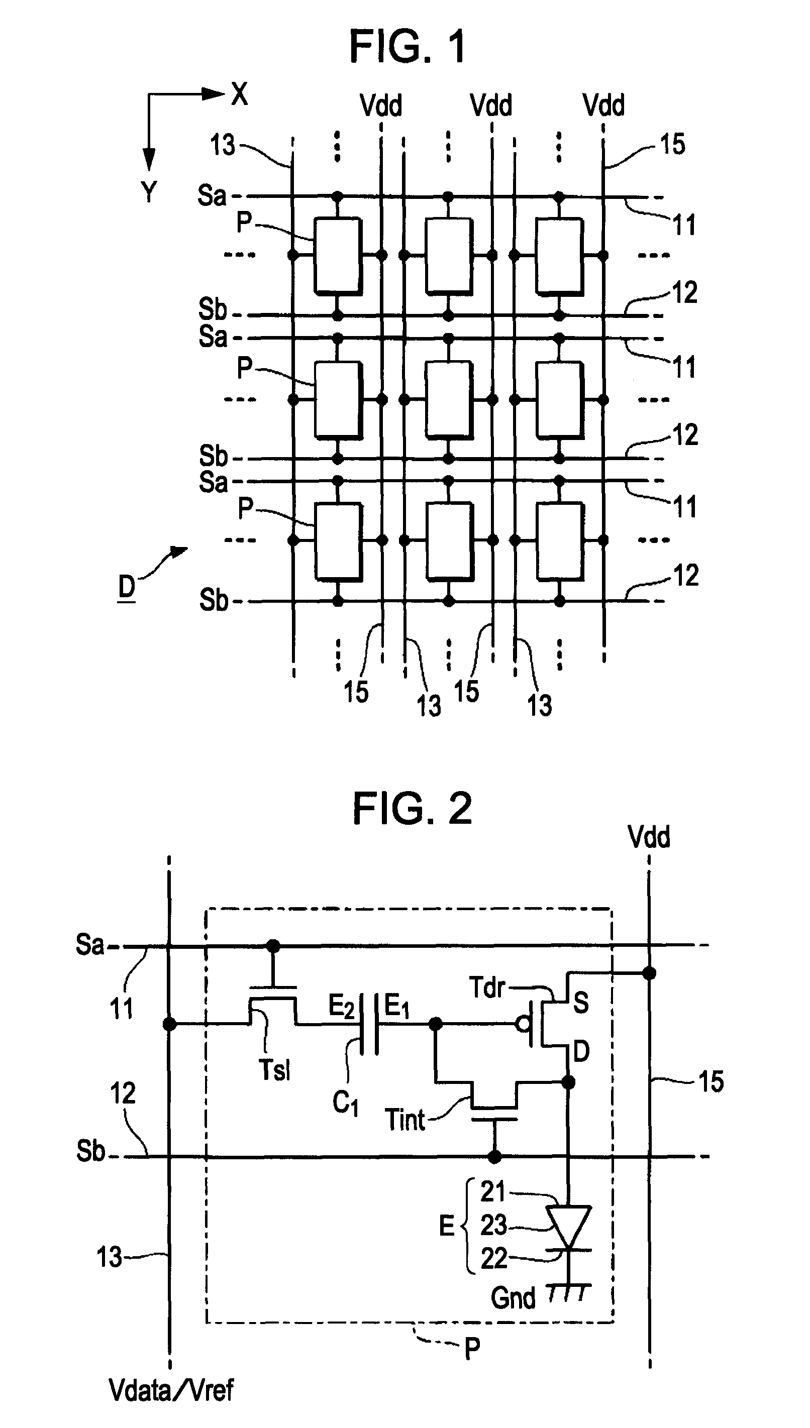
[0063]The components, such as the drive transistor Tdr and the light-emitting element E, of the unit element P shown in FIG. 2 are formed, as shown in FIG. 4, on the surface of a substrate 10. The substrate 10 is a planar member composed of an insulating material, such as glass or plastic. When forming the components of the unit element P on the surface of the substrate 10, an insulating film, such as a silicon oxide or silicon nitride film, covering the substrate 10 may b...

second embodiment

Modified Examples of Second Embodiment

[0124]A modified example of the above-described second embodiment is as follows. FIG. 17 is a plan view illustrating the unit element P in the processing step shown in FIG. 14 in which the first insulating layer L1 is formed. In the second embodiment, the gate electrode 521 of the drive transistor Tdr is extended in the Y direction. In this modified example, however, as shown in FIG. 17, the gate electrode 521 of the drive transistor Tdr is extended in the x direction. In this modified example, elements similar to those of the second embodiment are designated with like reference numerals, and an explanation thereof is thus omitted.

[0125]The intermediate conductor 52 of this modified example includes an interconnecting portion 525 extending from the top left of the electrode E1 toward the negative side in the Y direction and the gate electrode 521 which extends in the x direction from interconnecting portion 525 and which is overlapped with the s...

modified examples

[0130]Various modifications can be made to the above-described embodiments. Specific modified examples are as follows. The following modified examples may be combined if necessary.


PUM


Abstract

A light-emitting device includes a drive transistor that controls a current to be supplied to a light-emitting element from a power supply line, an electrical continuity portion that electrically connects the drive transistor with the light-emitting element, an initializing transistor that is turned ON to diode-connect the drive transistor, and a connecting portion that electrically connects the drive transistor with the initializing transistor. The power supply line includes a first portion extending in a predetermined direction. The electrical continuity portion and the connecting portion are formed from the same layer as that of the power supply line and are located on one side along the width of the first portion across the drive transistor.

Description

CROSS-REFERENCE TO RELATED APPLICATION[0001]The present application claims priority from Japanese Patent Application No. 2005-345299, filed in the Japanese Patent Office on Nov. 30, 2005, the entire disclosure of which is hereby incorporated by reference in its entirety.BACKGROUND[0002]1. Technical Field[0003]The present invention relates to a structure of a light-emitting device utilizing a light-emitting material, such as an organic electroluminescent (EL) material.[0004]2. Related Art[0005]As one type of active matrix light-emitting device, a structure in which a transistor that controls a current to be supplied to a light-emitting element (such a transistor is hereinafter referred to as a “drive transistor”) is provided for each light-emitting element is known. Another type of active matrix-light emitting device is disclosed in U.S Pat. No. 6,229,506 (FIG. 2) and JP-A-2004-133240 (FIGS. 2 and 3). In this structure, a transistor that compensates for errors of the threshold voltag...

Claims


Application Information

Patent Timeline
Patent Type & Authority Patents(United States)
IPC IPC(8): H01L29/72H05B44/00
CPCH01L27/12H05B33/08H01L27/3279H01L27/326H05B45/00H05B44/00H10K59/121H10K59/1315H05B33/26
Inventor KUBOTA, TAKEHIKOKANDA, EIJINOZAWA, RYOICHI
Owner SEIKO EPSON CORP
Why Eureka
Try Eureka