Multilayer printed wiring board

a printing board and wiring board technology, applied in the direction of printed element electric connection formation, non-metallic protective coating application, dielectric characteristics, etc., can solve the problems of high temperature of printed wiring board, low-elasticity layer separation, conductor stress, etc., to enhance the handle ability of resin composition

Active Publication Date: 2009-02-24
IBIDEN CO LTD +1
View PDF15 Cites 12 Cited by
  • Summary
  • Abstract
  • Description
  • Claims
  • Application Information

AI Technical Summary

Benefits of technology

[0006]The present invention has been made in order to solve the above problems, and an object of the invention is to provide a multilayer printed wiring board in which separation of a low-elasticity layer can be prevented even under high temperature and connection reliability of conductor posts penetrating through the low-elasticity layer can be secured.
[0023]In the multilayer printed wiring board, it is preferable that the diameter of the conductor post exceeds 30 μm. This condition can suppress voltage drop when power is supplied to the installed electrical parts, and prevent malfunction of the electrical parts. Furthermore, the electrical resistance of the conductor post can be suppressed to low levels. In the case of an IC chip having electrical parts of 1 GHz or less, voltage drop hardly occurs even when the conductor post is designed to be 30 μm in diameter. However, in the case of a high-speed IC chip of 3 GHz or more, the voltage drop is remarkable, and thus it is preferable that the diameter of the conductor post exceeds 30 μm. When the thickness of the conductor post is not uniform, it is preferable that the diameter of the narrowest part of the conductor post exceeds 30 μm. This is because the conductor resistance of the conductor post is reduced or the resistance to fatigue degradation and the resistance to a heat cycle are enhanced. It is preferable that the diameter of the conductor post is more than 30 μm and not more than 60 μm.

Problems solved by technology

However, when a thermal treatment process is executed to make a printed wiring board or the printed wiring board is actually used, the temperature of the printed wiring board exceeds the Tg due to heating of an IC chip operating in a high frequency region, etc., in some cases.
), and thus there occurs such a problem that separation is likely to occur between the printed wiring board and the low-elasticity layer.
Furthermore, in the high-temperature region, the low-elasticity layer expands significantly more as compared with the conductor penetrating via the low-elasticity layer, and thus there is a problem that the conductor suffers stress and thus it is liable to be broken.
Particularly when an IC having an operating clock in a high frequency region (for example, 3 GHz or more) is mounted, this problem is more remarkable due to heat.

Method used


Image

  • Multilayer printed wiring board
  • Multilayer printed wiring board
  • Multilayer printed wiring board

Examples


examples

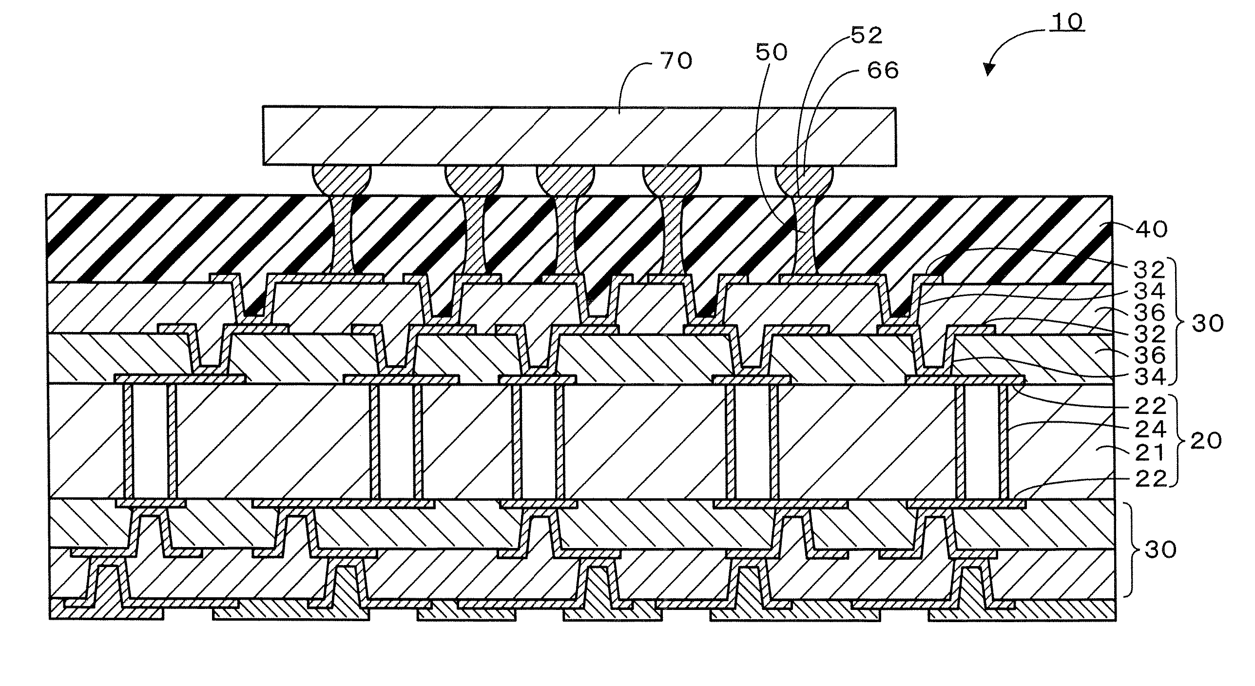
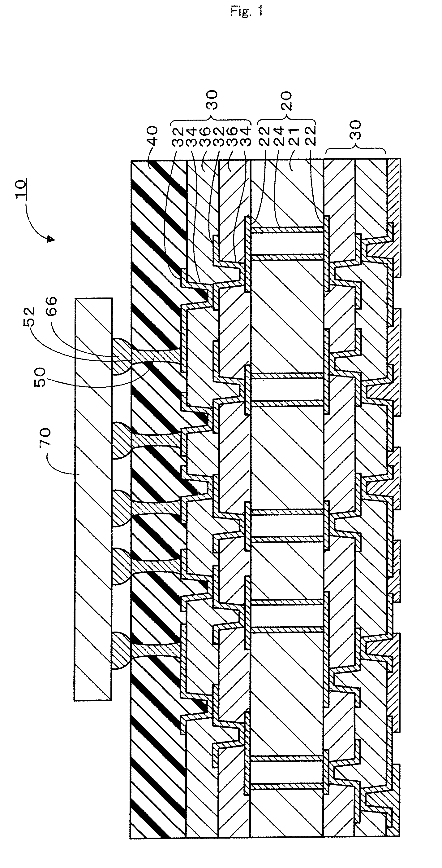
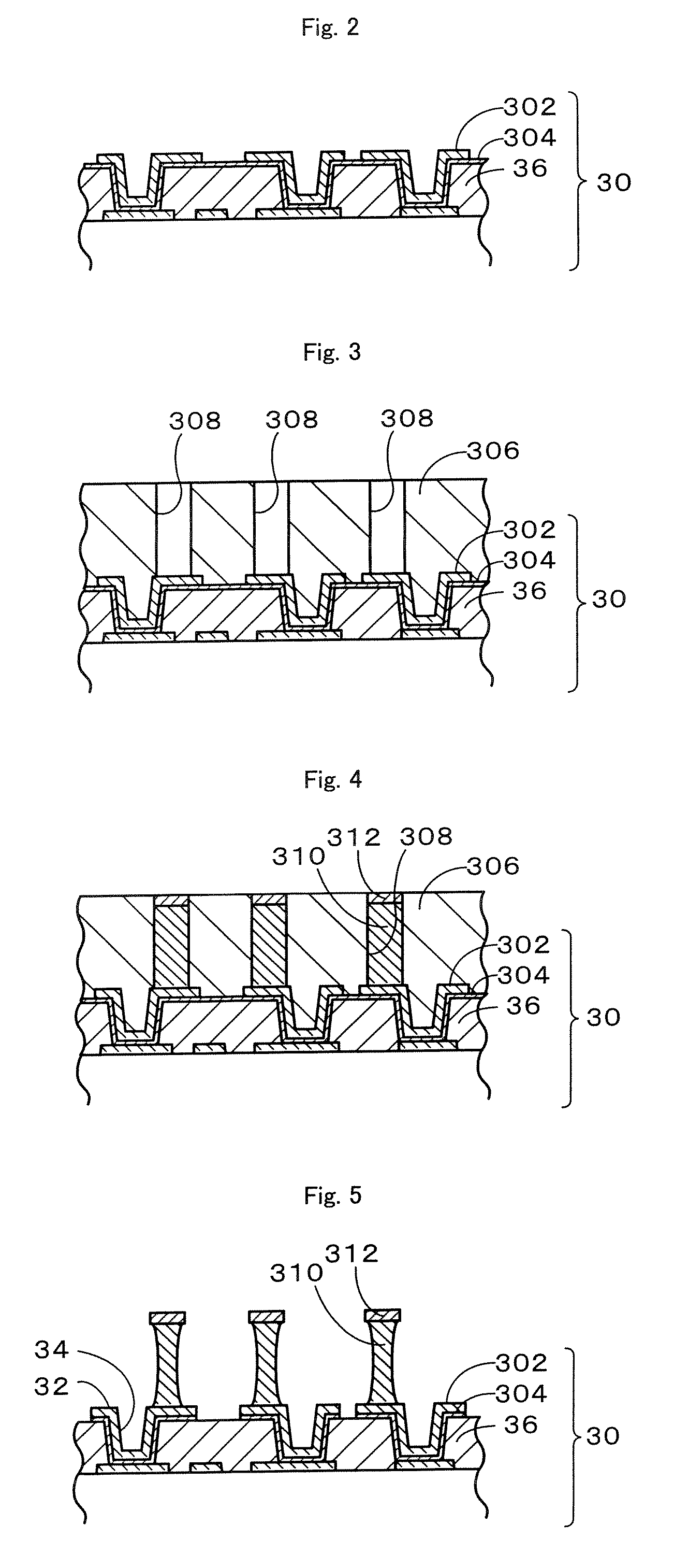
[0061]Examples to verify the effect of the multilayer printed wiring board 10 of the above-described embodiment will be described. First, the relationship between the aspect ratio Rasp of the conductor post and the variation rate of the electrical resistance when heating / cooling is repeated will be described. In this case, the multilayer printed wiring board having the conductor posts of the first to twelve examples shown in the table of FIG. 9 were prepared according to the above-described embodiment. Specifically, in each example, the hole diameter of the opening 308 formed in the dry film 306 (240 μm in thickness) of FIG. 3 by using a carbon dioxide gas laser was set in conformity with the maximum diameter of the conductor post, and the etching time of the copper layer 310 of FIG. 5 was set in conformity with the minimum diameter of the conductor post. When the minimum diameter is equal to the maximum diameter, the conductor post is a substantially straight columnar post. When th...


PUM


Abstract

A multilayer printed wiring board is equipped with a core board 20, a build-up layer 30 formed on the core board 20 so as to have a conductor pattern 32 on the upper surface thereof, a low-elasticity layer 40 formed on the build-up layer 30, lands 52 that are provided on the upper surface of the low-elasticity layer 40 and connected to an IC chip 70 via solder bumps 66, and conductor posts 50 that penetrate through the low-elasticity layer 40 and electrically connect the lands 52 to the conductor pattern 32. The low-elasticity layer 40 is formed of resin composition containing epoxy resin, phenol resin, cross-linked rubber particles and a hardening catalyst.

Description

Cross-Reference to Related Applications[0001]The present invention is a continuation of International Application No. PCT / JP2005 / 010099, filed on May 26, 2005, which claims priority from Japanese Patent Application No. 2004-157459, filed on May 27, 2004.TECHNICAL FIELD[0002]The present invention relates to a multilayer printed wiring board.BACKGROUND ART[0003]High functionalization and miniaturization have been remarkable for electronic equipment represented by portable information terminals and communications terminals. A flip chip system in which IC chips are directly mounted on the surface of a multilayer printed wiring board has been adopted as a manner of mounting IC chips used for these electronic equipment on a multilayer printed wiring board in high density. One known multilayer printed wiring board is equipped with a core board, a build-up layer formed on the core board, and mounting electrodes on which an IC chip is mounted via soldering bumps on the upper surface of the b...

Claims


Application Information

Patent Timeline
Patent Type & Authority Patents(United States)
IPC IPC(8): H01L23/14H01L23/28H01L21/60H01L23/12H01L23/498H05K1/02H05K3/28H05K3/40H05K3/46
CPCH01L23/49811H01L23/49822H05K1/0271H05K1/0373H05K1/115H01L23/49816H01L2224/16235H01L2224/16H01L2924/01046H01L2924/01078H01L2924/01079H05K3/28H05K3/4007H05K3/4602H05K2201/0133H05K2201/0367H05K2201/10674H01L2924/01019H01L2924/01068H05K2201/068H01L23/12H05K3/46
Inventor KARIYA, TAKASHIFURUTANI, TOSHIKIGOTO, HIROFUMIIWANAGA, SHIN-ICHIRO
Owner IBIDEN CO LTD
Why Eureka
Try Eureka