Photovoltaic power device and manufacturing method thereof

a photovoltaic power and power device technology, applied in the field of photovoltaic power devices, can solve the problems of limiting the reflection ratio, and achieve the effects of reducing the reflection ratio of incident sunlight, low resistance, and photoelectric conversion

Inactive Publication Date: 2011-02-17
MITSUBISHI ELECTRIC CORP
View PDF7 Cites 13 Cited by
  • Summary
  • Abstract
  • Description
  • Claims
  • Application Information

AI Technical Summary

Benefits of technology

[0013]According to the present invention, the first diffusion layer of a low resistance is formed at a light-receiving surface side of a silicon substrate, and concave portions are provided at a predetermined interval such that not the whole of the first diffusion layer is removed, and the third diffusion layer having an impurity concentration lower than that of the first diffusion layer is provided in a range of a predetermined depth from a surface of the concave portions. Therefore, by decreasing the reflection ratio of incident sunlight, a photoelectric conversion can be efficiently performed in the third diffusion layer within the concave portions, and a photocurrent generated by the photoelectric conversion can be caused to reach surface electrodes via the first diffusion layer on a silicon substrate surface having a low resistance. Because the photocurrent is collected by surface electrodes through the first diffusion layer having a low resistance, a resistance loss can be suppressed, a forming area of the surface electrodes can be reduced by expanding an interval between the surface electrodes, and more sunlight can be taken into the silicon substrate. As a result, the photoelectric conversion efficiency can be improved more than that of conventional techniques without degrading the efficiency of extracting a photocurrent to an external circuit.

Problems solved by technology

Because of this problem, there is a limit in reducing the reflection ratio in the case of the polycrystalline silicon substrate.

Method used


Image

  • Photovoltaic power device and manufacturing method thereof
  • Photovoltaic power device and manufacturing method thereof
  • Photovoltaic power device and manufacturing method thereof

Examples


first embodiment

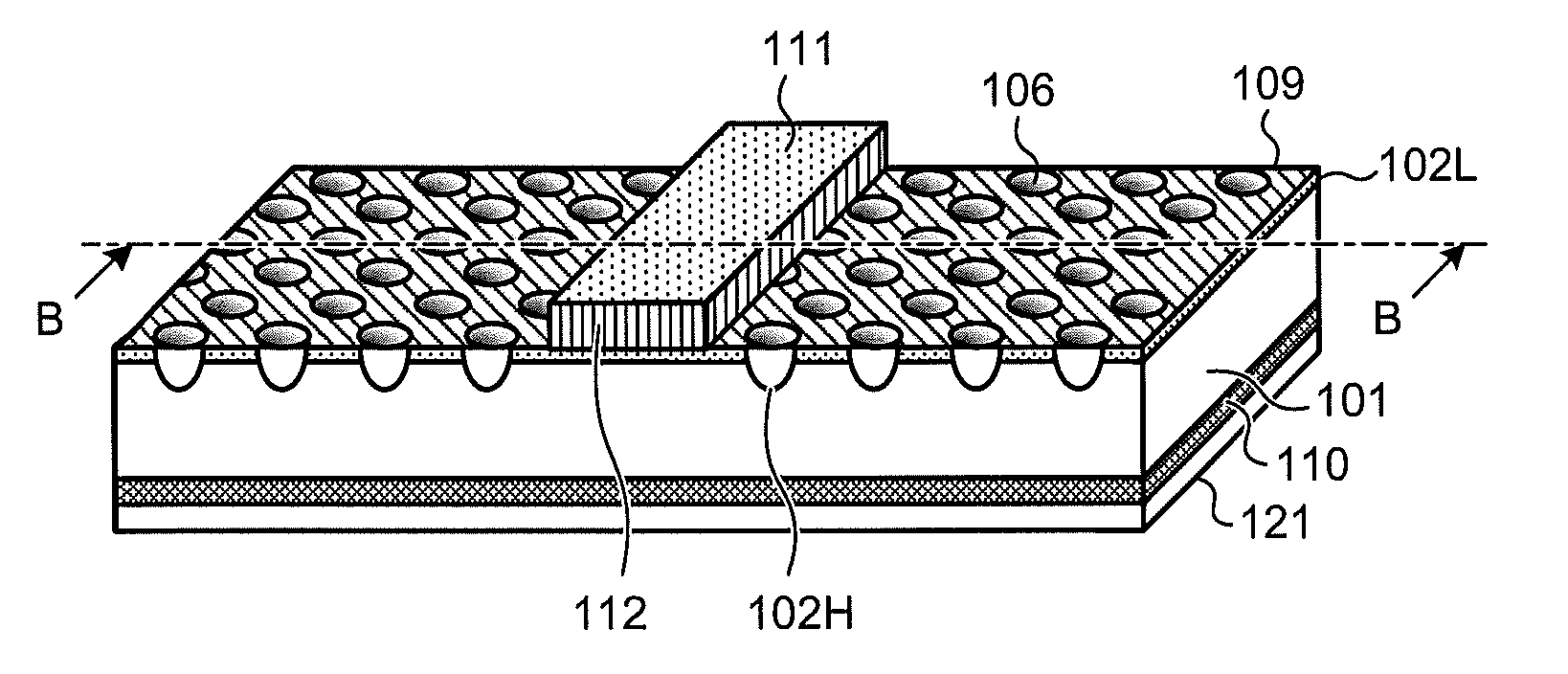
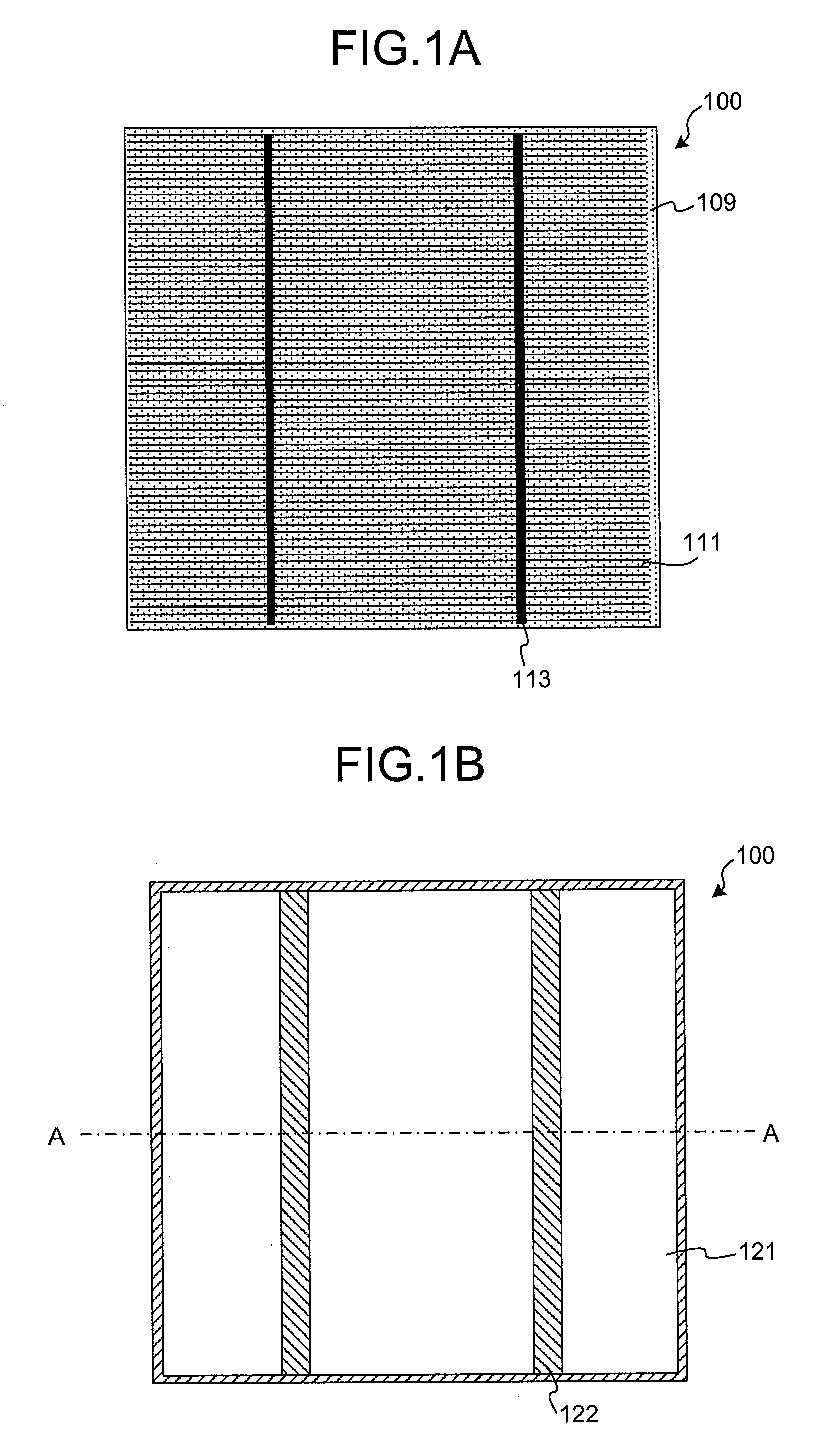
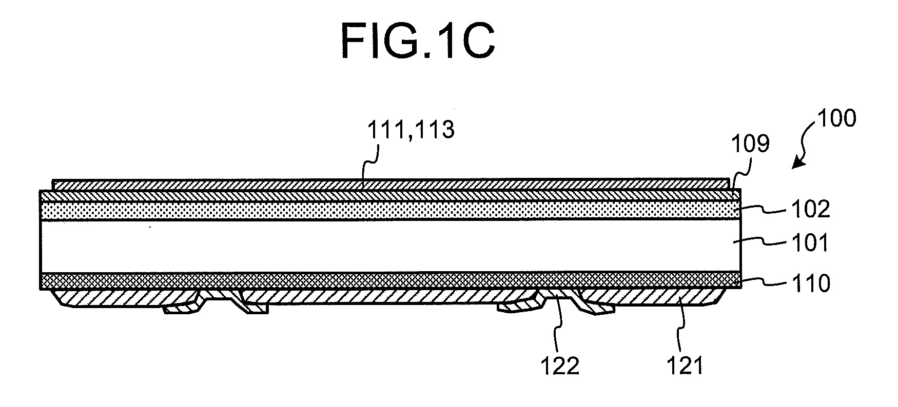
[0075]First, prior to explanations of a configuration of a photovoltaic power device according to a first embodiment of the present invention, an outline of an entire configuration of a general photovoltaic power device is explained. FIGS. 1A to 1C are schematic views of an example of an entire configuration of a general photovoltaic power device, where FIG. 1A is a top view of the photovoltaic power device, FIG. 1B is a back view of the photovoltaic power device, and FIG. 1C is a cross-sectional view along A-A in FIG. 1B. A photovoltaic power device 100 includes a photoelectric conversion layer including a P-type silicon substrate 101 as a semiconductor substrate, an N-type diffusion layer 102 diffused with an N-type impurity formed on a surface at one principal surface (a light receiving surface) side of the P-type silicon substrate 101, and a P+ layer 110 containing a P-type impurity in a higher concentration than that of the silicon substrate 101 formed on a surface at a side of...

second embodiment

[0102]In the explanations of the first embodiment, after the high-resistance N-type diffusion layer 102H is formed within the concave portions 106 in FIG. 5G and FIG. 6G, the phosphorus glass layer in the low-resistance N-type diffusion layer 102L and on the high-resistance N-type diffusion layer 102H is removed in the hydrofluoric acid solution. Alternatively, the uppermost surface of the low-resistance N-type diffusion layer 102L and the high-resistance N-type diffusion layer 102H can be etched with a mixed liquid of hydrofluoric acid and nitric acid. The following process procedures are identical to those described in the first embodiment and thus explanations thereof will be omitted.

[0103]According to the second embodiment, after etching the phosphorus glass layer in the low-resistance N-type diffusion layer 102L and on the high-resistance N-type diffusion layer 102H, the uppermost surface of the diffusion layers 102L and 102H is etched with a mixed liquid of hydrofluoric acid a...

third embodiment

[0104]In the third embodiment, there is explained a case of forming openings in a method different from that of the first embodiment. FIG. 9 is an example of a configuration of a laser processing apparatus used to form openings of the third embodiment. The laser processing apparatus 200B includes the stage 201 on which an object to be processed such as the silicon substrate 101 is mounted, the laser oscillator 203 that outputs the laser beam 204, a first galvanomirror 211 that is arranged between the stage 201 and the laser oscillator 203 and guides the laser beam 204 to an optical path while scanning in an X-axis direction 212, and a second galvanomirror 213 that guides the laser beam 204 reflected by the first galvanomirror 211 to the optical path while scanning in a Y-axis direction 214.

[0105]In the laser processing apparatus 200B having this configuration, the laser beam 204 collected in a spot shape is irradiated to a predetermined position of the etching resistance film 103 on...


PUM


Abstract

A photovoltaic power device includes a P-type silicon substrate, a low-resistance N-type diffusion layer diffused with an N-type impurity in a first concentration formed at a light-incidence surface side, grid electrodes formed on the low-resistance N-type diffusion layer, a P+ layer formed on a back surface, and a back surface electrode formed on the P+ layer. The photovoltaic power device has concave portions provided at a predetermined interval to reach the silicon substrate from an upper surface of the low-resistance N-type diffusion layer, and an upper surface of a region between adjacent concave portions includes the low-resistance N-type diffusion layer. A high-resistance N-type diffusion layer diffused with an N-type impurity in a second concentration, which is lower than the first concentration, is formed in a range of a predetermined depth from a formation surface of the concave portions.

Description

TECHNICAL FIELD[0001]The present invention relates to a photovoltaic power device and a manufacturing method thereof.BACKGROUND ART[0002]To improve the performance of photovoltaic power devices such as solar batteries, as to how efficiently sunlight is to be taken into inside of a photovoltaic power device is an important factor. Therefore, conventionally, a texture structure having intentionally formed a fine uneven concavo-convex shape in a size of dozens of nanometers to dozens of micrometers on a surface of a light incidence side is manufactured. In this texture structure, light once reflected on a surface is made to enter the surface again to take more sunlight into the inside of the photovoltaic power device, thereby increasing a generated current and improving its photoelectric conversion efficiency.[0003]As a method of forming a texture structure on a solar battery substrate, when a substrate is a monocrystalline silicon (Si) substrate, an anisotropic etching process using a...

Claims


Application Information

Patent Timeline
Patent Type & Authority Applications(United States)
IPC IPC(8): H01L31/0236H01L31/18H01L31/068
CPCH01L31/02363H01L31/03529H01L31/18H01L31/1804Y02E10/547H01L31/068Y02P70/50
Inventor ISHIHARA, TAKASHINISHIMURA, KUNIHIKO
Owner MITSUBISHI ELECTRIC CORP
Why Eureka
Try Eureka