Package systems having interposers

a technology of interposers and packaging systems, applied in the direction of semiconductor devices, semiconductor/solid-state device details, electrical apparatus, etc., can solve the problems of minimum size needed to make these components, physical limits of the density that can be achieved in two dimensions, and the requirement of more complex designs

Active Publication Date: 2011-11-24
TAIWAN SEMICON MFG CO LTD
View PDF16 Cites 144 Cited by
  • Summary
  • Abstract
  • Description
  • Claims
  • Application Information

AI Technical Summary

Problems solved by technology

Although dramatic improvements in lithography have resulted in considerable improvements in 2D integrated circuit formation, there are physical limits to the density that can be achieved in two dimensions.
One of these limits is the minimum size needed to make these components.
Also, when more devices are put into one chip, m

Method used


Image

  • Package systems having interposers
  • Package systems having interposers
  • Package systems having interposers

Examples


Embodiment Construction

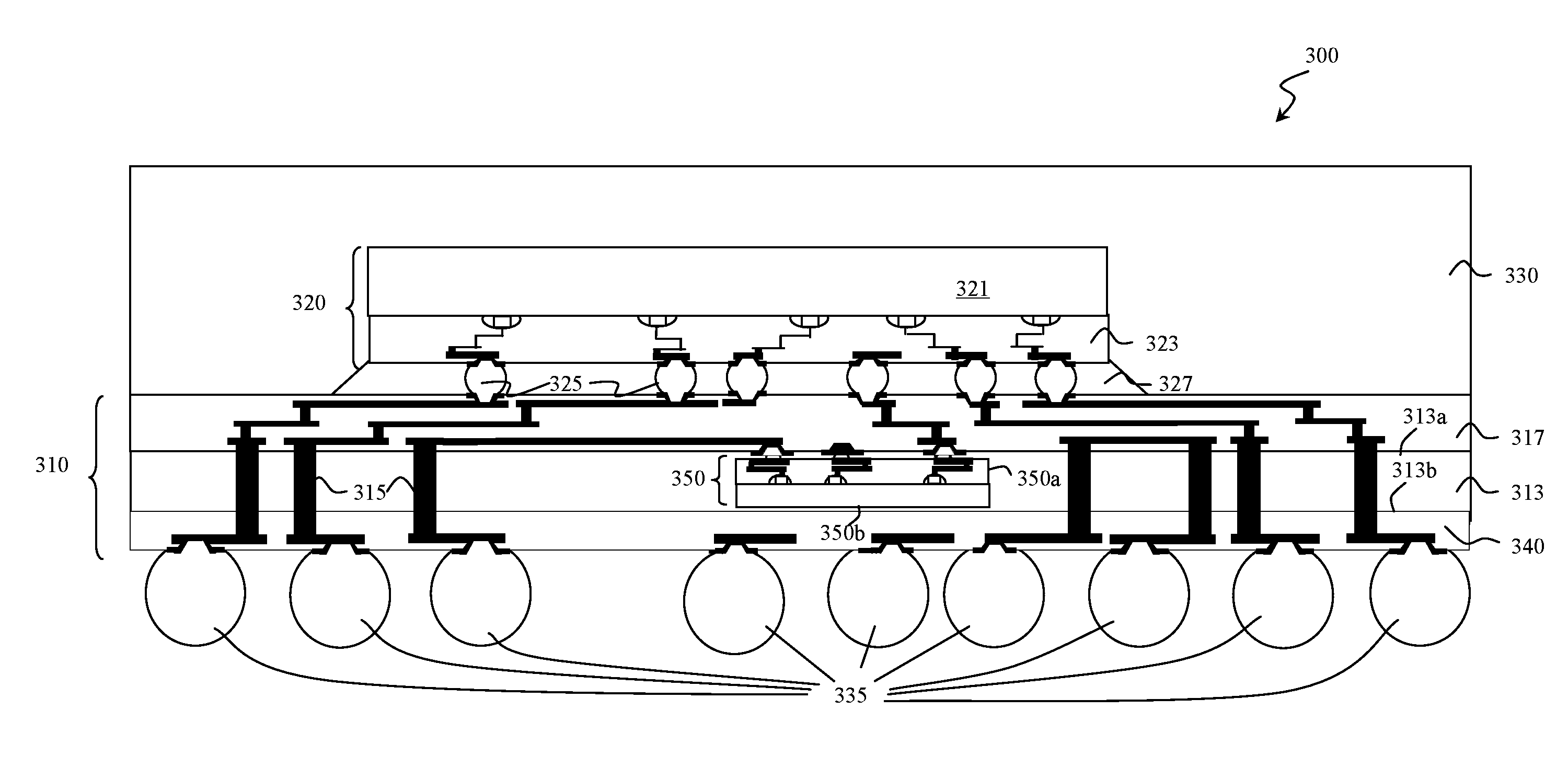
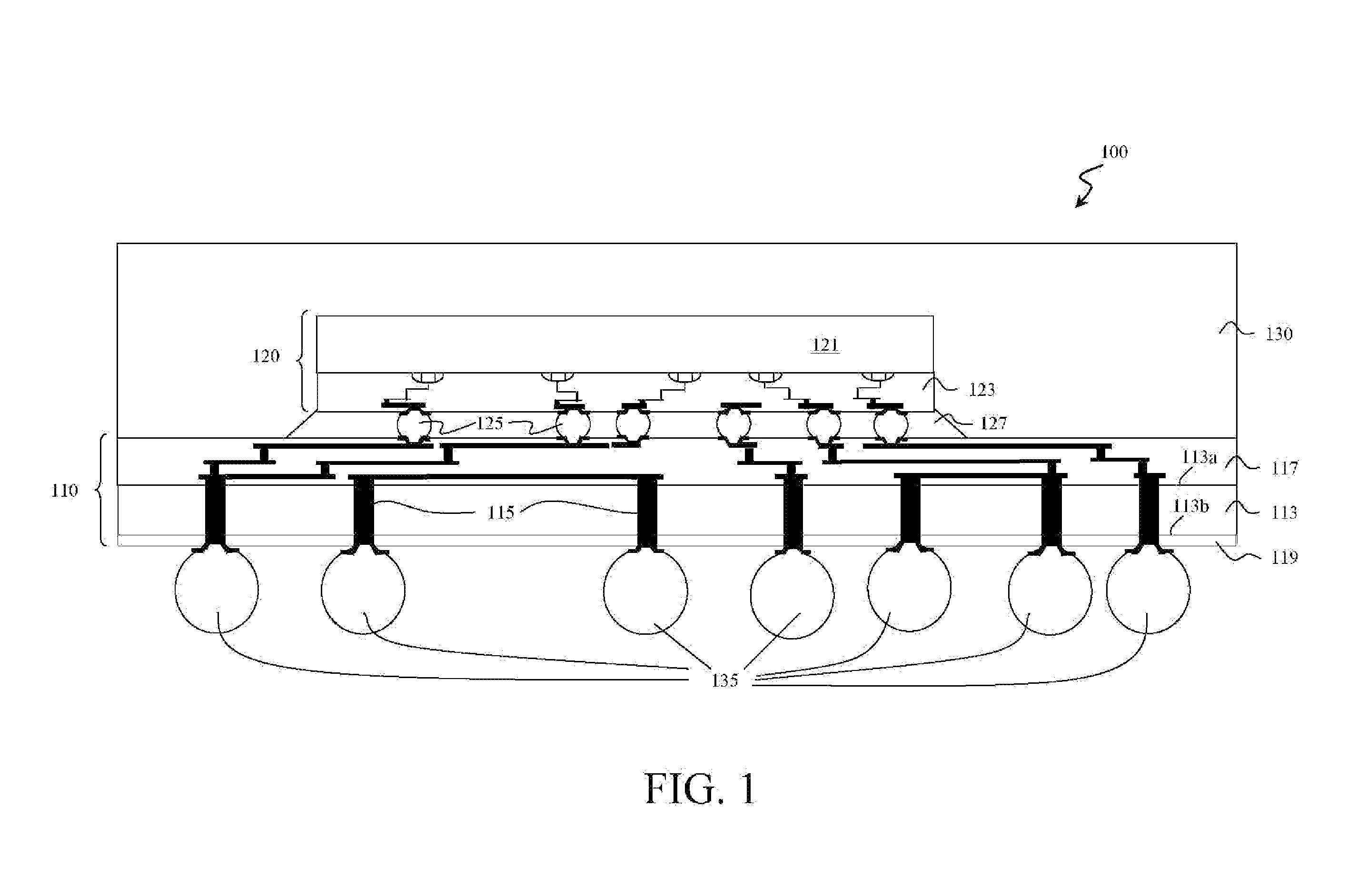
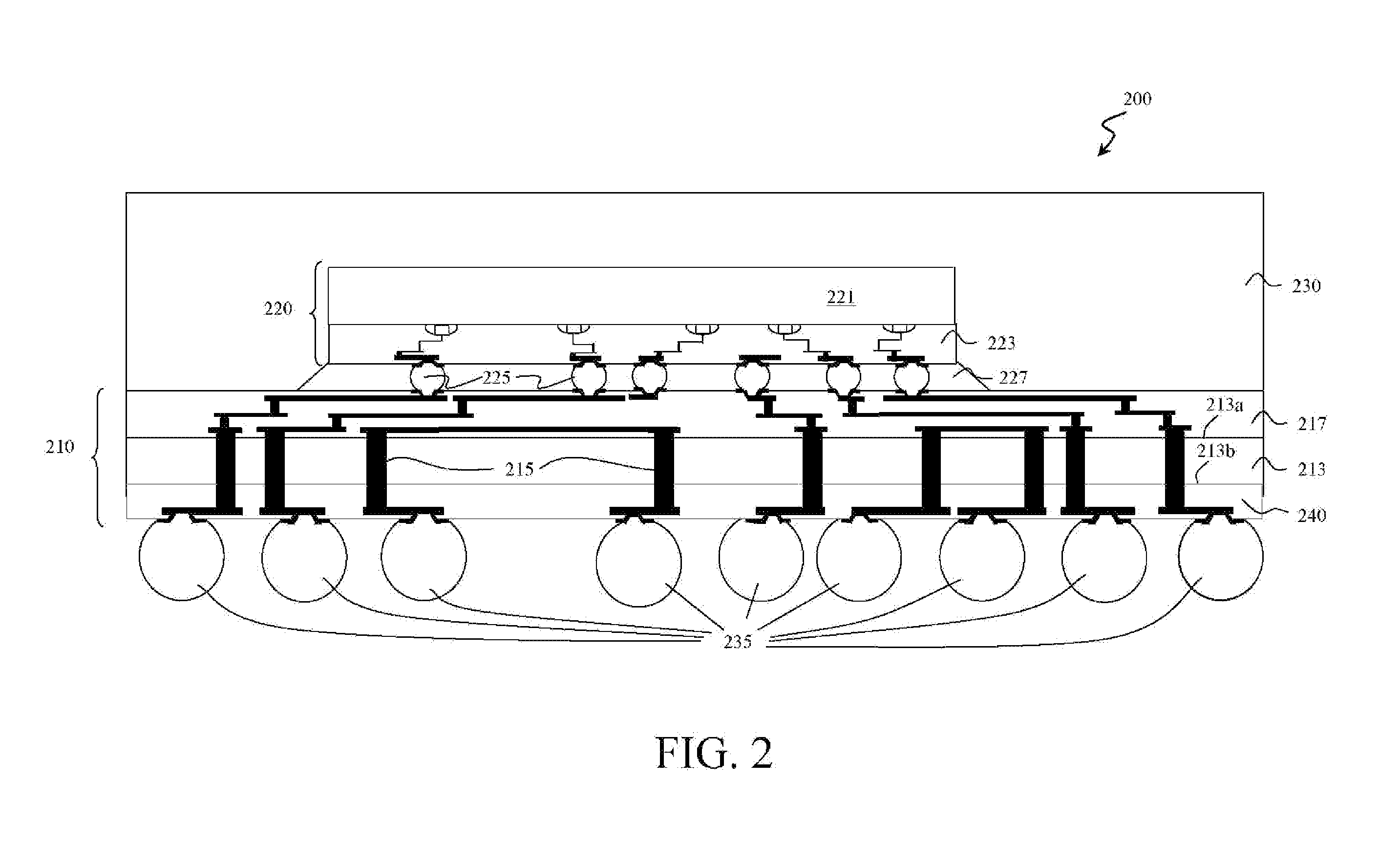
[0017]Conventionally, a package system has a silicon interposer disposed between a silicon die and an organic substrate. The silicon interposer has a plurality of through-silicon-via (TSV) structures for an electrical connection between the silicon die and the organic substrate. The formation of the TSV structures includes various processes, such as a TSV etch process, a barrier / seed layer deposition process, a copper plating process, a chemical-mechanical-polish (CMP) process for removing portions of the copper layer and barrier / seed layer, and / or other semiconductor processes. The formation of the TSV structures in the silicon interposer increases the cost of manufacturing the package system. It is found that a polyimide cap layer covering the silicon die is disposed over the silicon interposer. The applicants also found that a coefficient of thermal expansion (CTE) mismatch exists between the polyimide cap layer and the silicon interposer may result in an intermetal dielectric (I...


PUM


Abstract

A package system includes a first integrated circuit disposed over an interposer. The interposer includes at least one molding compound layer including a plurality of electrical connection structures through the at least one molding compound layer. A first interconnect structure is disposed over a first surface of the at least one molding compound layer and electrically coupled with the plurality of electrical connection structures. The first integrated circuit is electrically coupled with the first interconnect structure.

Description

TECHNICAL FIELD[0001]The present disclosure relates generally to the field of semiconductor package systems, and more particularly, to package systems having interposers.BACKGROUND OF THE DISCLOSURE[0002]Since the invention of integrated circuits, the semiconductor industry has experienced continual rapid growth due to continuous improvements in the integration density of various electronic components (i.e., transistors, diodes, resistors, capacitors, etc.). For the most part, this improvement in integration density has come from repeated reductions in minimum feature size, allowing for the integration of more components into a given area.[0003]These integration improvements are essentially two-dimensional (2D) in nature, in that the volume occupied by the integrated components is essentially on the surface of the semiconductor wafer. Although dramatic improvements in lithography have resulted in considerable improvements in 2D integrated circuit formation, there are physical limits...

Claims


Application Information

Patent Timeline
IPC IPC(8): H01L23/538
CPCH01L21/4846H01L21/56H01L2924/1305H01L2924/15192H01L2224/0239H01L21/768H01L24/03H01L24/11H01L24/19H01L2224/02331H01L2224/02372H01L2224/0401H01L2924/13091H01L2924/10253H01L2924/15311H01L2224/32225H01L21/563H01L21/565H01L23/295H01L23/3128H01L23/49816H01L23/49822H01L23/49827H01L23/5389H01L24/24H01L2224/16225H01L2224/24227H01L2224/73203H01L2224/73204H01L2924/01013H01L2924/0102H01L2924/01029H01L2924/01032H01L2924/01033H01L2924/01049H01L2924/01059H01L2924/01073H01L2924/01078H01L2924/01079H01L2924/01082H01L2924/01006H01L2924/01019H01L2924/01023H01L2924/01024H01L2924/01047H01L2924/01074H01L2924/10329H01L2924/01327H01L2924/00012H01L2924/00H01L2924/15788H01L2224/12105H01L2924/181H01L2924/12042H01L2924/14H01L21/4853H01L21/4857H01L21/486H01L21/6835H01L25/0657H01L25/50H01L2221/68359H01L2225/06517H01L2225/06548H01L2225/06572
Inventor LIN, YUNG-CHILIN, JING-CHENGYU, CHEN-HUA
Owner TAIWAN SEMICON MFG CO LTD
Why Eureka
Try Eureka