
Pulse Control For NonVolatile Memory

a nonvolatile memory and pulse control technology, applied in the field of pulse control for nonvolatile memory, can solve the problems of difficult generation of discrete pulses that are effective for these purposes, stable defect structure, and difficult annealing or repair,

Active Publication Date: 2011-11-24
RAMBUS INC
View PDF7 Cites 28 Cited by
  • Summary
  • Abstract
  • Description
  • Claims
  • Application Information

AI Technical Summary

Problems solved by technology

The defect structure is stable and difficult to anneal or repair, but the defect precursors may be removed or annealed if the stress condition is removed for a periodic “resting” between periods of stress.
It is difficult to generate discrete pulses that are effective for these purposes, especially for arrays which are divided into pages of many thousands of cells that are programmed or erased as a unit (e.g., flash memory cells and SONOS cells).
The loading provided by internal conductor routing and transistors used in these designs result in slow pulse rise times, making it difficult to generate short term, discrete pulses; that is to say, the rise times for voltage pulses used for programming and erasing of these memory types is sufficiently slow that it is difficult to generate high-voltage, short term pulses that can be effectively used to retard defect formation during memory cell state change operations.
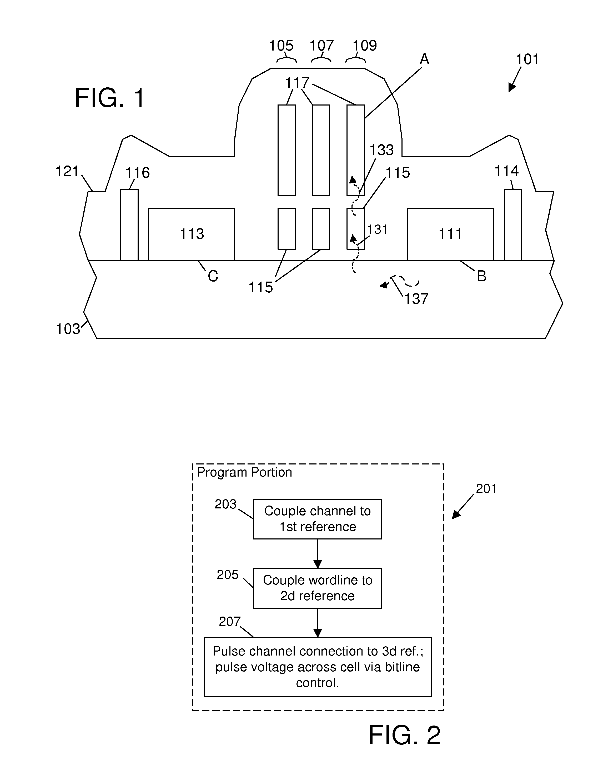
It is within the second gap 133 that large electric fields can primarily cause problems that increase leakage and so affect the ability of a memory cell to set and reset (program / erase) in a repeatable manner.
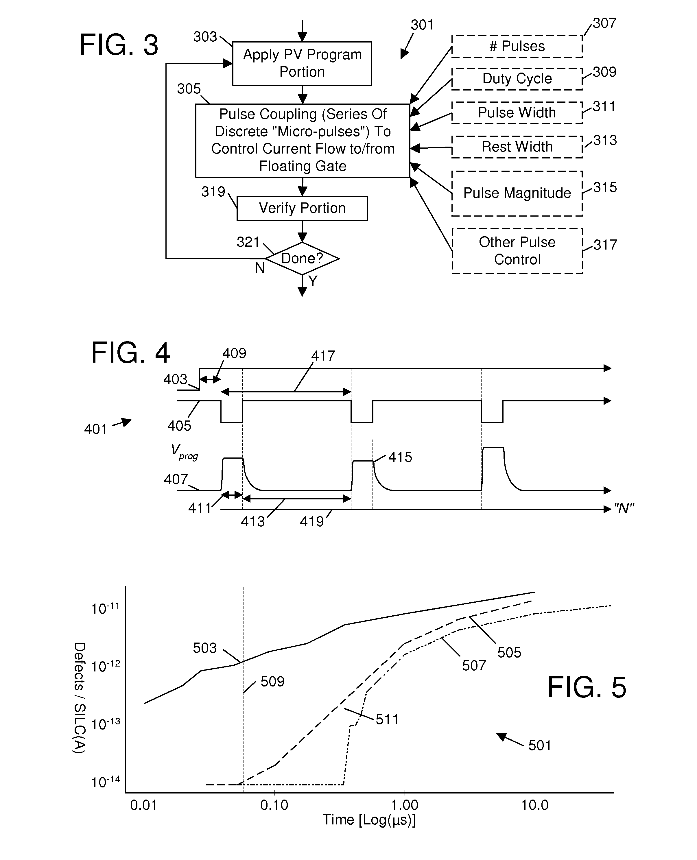
As mentioned previously, this result is difficult to achieve through wordline control, and bitline control is effectively applied by the embodiments of FIGS. 1-4 in order to obtain voltage pulses “fast enough” to obtain the benefits represented by the data of FIG. 5.
These alternatives are not the only options available to a skilled designer.
This time may be too long to be able to effectively use bitline control alone to generate voltage pulses of 50 nanoseconds or less using bitline control.
However, certain types of memory devices may also be damaged during the application of forming voltages or other conditioning events to prepare devices for first use.
Because larger-than-normal currents or longer-than-normal currents may flow through memory cells during these “conditioning events,” the memory cells are even more susceptible to the formation of undesired defects.
These issues make it more difficult to use wordline control to generate robust voltage pulses, but wordline control is nevertheless possible.

Method used


Image

  • Pulse Control For NonVolatile Memory
  • Pulse Control For NonVolatile Memory
  • Pulse Control For NonVolatile Memory

Examples


first embodiment

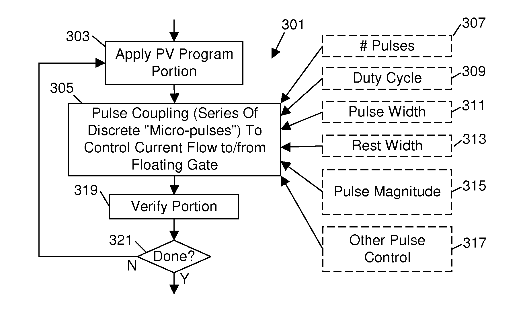
[0029]A first embodiment presented by this disclosure provides a method of controlling a bitline of a memory cell in order to limit electric field times so as to inhibit defect formation; an associated structure is also provided. The design philosophy adopted by embodiments based on bitline control is that wordline voltage should be held relatively constant (e.g., wordline control separated from application of a multiple pulses to effectuate a single program cycle) and a bitline should be pulsed between ground and another reference voltage to turn off programming (or other voltage activities) and provide a rest state. Because a bitline presents reduced loading issues relative to other conductors in a flash memory device (as the bitline is typically fabricated from a metal, e.g., copper), pulsed operations discussed herein may be effectively applied to substantially shorten pulse rise time. Simply stated, using bitline control helps facilitate short duration voltage pulses, potential...

second embodiment

[0051]FIG. 9 presents block diagram 901 of one implementation of to bitline control in a flash memory device. In particular, two basic elements are illustrated in FIG. 9, including control logic 903 and a page buffer 905; the memory array itself is not illustrated so as to explain some of the control functions associated with the device. The control logic handles functions associated with switching, voltage control and associated timing for the memory array; these functions are illustrated by several logic blocks in FIG. 9. This control logic is generically connected to the device (e.g., to supply a write data register (“WDR”) 915, bitline drivers 917 and sense amplifiers 921), though it should be understood that individual logic elements depicted (designated by numerals 907, 909, 911 and 913) may in fact electrically connect to and control only specific elements within the device, e.g., to the memory array, sense amplifier, WDR, or only to other logic elements. A state machine 907 ...


PUM


Abstract

This disclosure provides a nonvolatile memory device that uses pulsed control and rest periods to mitigate the formation of defect precursors. A first embodiment uses pulsed bitline control, where the coupling between a memory cell channel and a reference voltage (selected in response to the bitline) is pulsed when it is desired to change state in the associated memory cell. Each pulse may be chosen to be less than about (20) nanoseconds, while a “rest period” between pulses typically is chosen to be on the order of about a hundred nanoseconds or greater (e.g., one microsecond). Because bitline control is used, very short rise times can be enabled, enabling generation of pulse durations of (50) nanoseconds or less. In other embodiments, these methods may also be more generally applied to other conductors (e.g., wordline or substrate well, for program or erase operations); if desired, segmented wordlines or bitlines may also be used, to minimize RC loading and enable sufficiently short rise times to make pulses robust.

Description

BACKGROUND[0001]Nonvolatile memory can retain stored information without the continual requirement of short-interval refresh operations, i.e., such that memory contents can be retained in the absence of external power for at least as long as typical on / off times of electronic devices; for these reasons, nonvolatile memory can save power, enable new applications and further extend functionality of portable devices.[0002]To date, one of the most cost-effective forms of nonvolatile memory is flash memory, which unfortunately suffers from use-based degradation. That is to say, flash memory in particular eventually loses its ability to retain information for any length of time, with current expected lifetime being about 10,000-100,000 read and write cycles. It is believed that one primary cause of this life cycle wear is damage to the oxide layers in these devices from the formation of traps that arise under the influence of high electromagnetic fields used in programming (“setting”) and...

Claims


Application Information

Patent Timeline
IPC IPC(8): G11C16/04G11C16/12
CPCG11C16/10G11C16/3459G11C16/12G11C16/08G11C16/30G11C16/32G11C16/0408G11C16/26
Inventor KELLAM, MARK D.HAUKNESS, BRENT STEVENBRONNER, GARY B.DONNELLY, KEVIN
Owner RAMBUS INC
Learn More