Conductive sheet and capacitive touch panel

a capacitive touch panel and conductive sheet technology, applied in the direction of electronic switching, pulse technique, instruments, etc., can solve the problems of low current transfer rate, long response time, low response speed, etc., to improve touch position detection sensitivity, reduce the probability of complete disconnection, and improve visibility

Active Publication Date: 2011-12-01
FUJIFILM CORP
View PDF2 Cites 99 Cited by
  • Summary
  • Abstract
  • Description
  • Claims
  • Application Information

AI Technical Summary

Benefits of technology

[0014]In view of the above problems, an object of the present invention is to provide a conductive sheet and a capacitive touch panel, which can have a lower probability of complete disconnection between sensing sections

Problems solved by technology

Thus, when the conventional touch panel is used in the large device in the above future trend, the large-sized touch panel has a low current transfer rate between the electrodes, and thereby exhibits a low response speed

Method used


Image

  • Conductive sheet and capacitive touch panel
  • Conductive sheet and capacitive touch panel
  • Conductive sheet and capacitive touch panel

Examples


examples

[0290]The present invention will be described more specifically below with reference to Examples. Materials, amounts, ratios, treatment contents, treatment procedures, and the like, used in Examples, may be appropriately changed without departing from the scope of the present invention. The following specific examples are therefore to be considered in all respects as illustrative and not restrictive.

first example

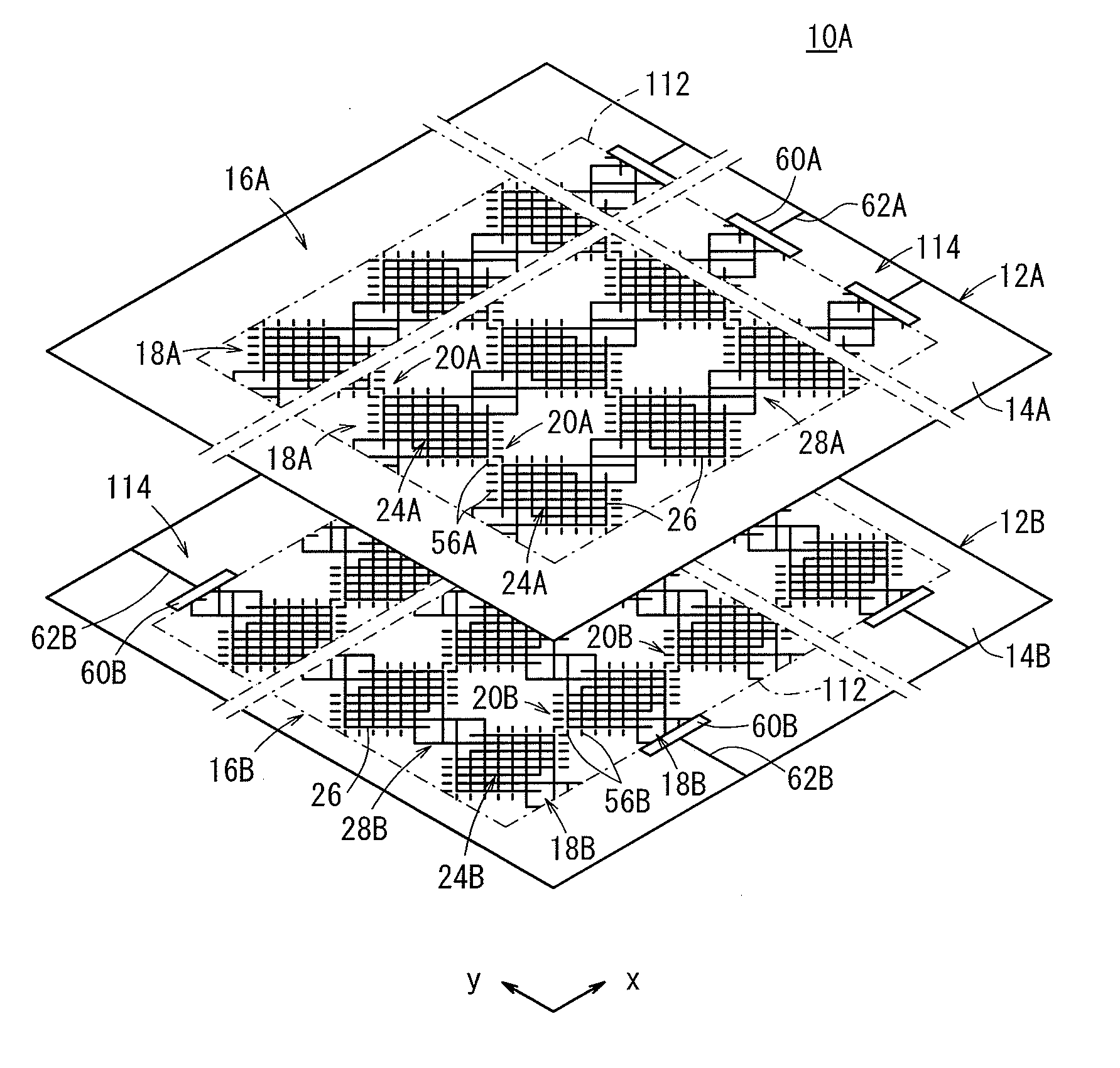
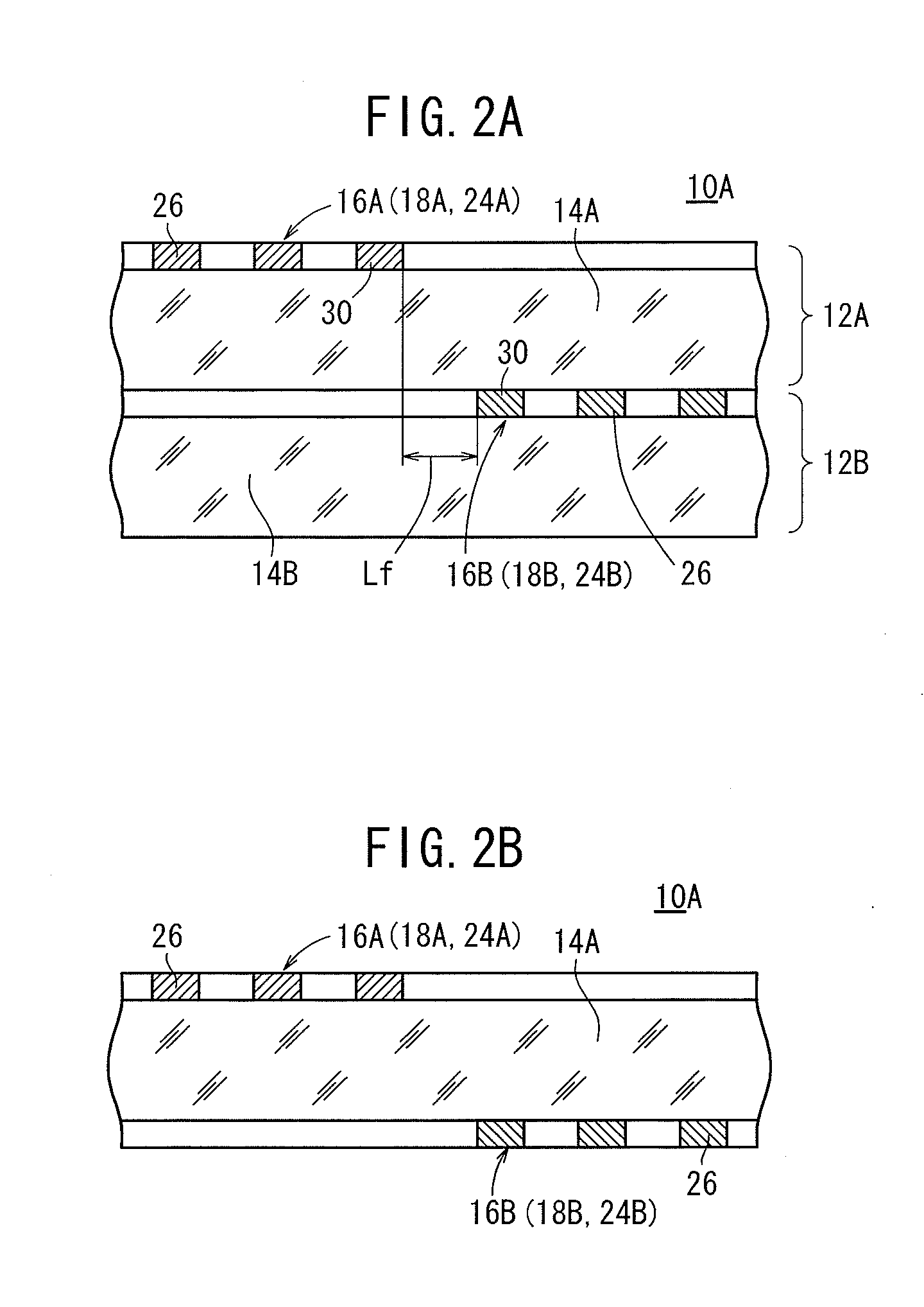
[0291]In First Example, 100 first conductive sheets 12A and 100 second conductive sheets 12B were produced by the following treatments. The thin metal wires had a line width of 1 μm, and the small lattices 26 had a side length of 100 μm.

(Photosensitive Silver Halide Material)

[0292]An emulsion containing an aqueous medium, a gelatin, and silver iodobromochloride particles was prepared. The amount of the gelatin was 10.0 g per 150 g of Ag, and the silver iodobromochloride particles had an I content of 0.2 mol %, a Br content of 40 mol %, and an average spherical equivalent diameter of 0.1 μm.

[0293]K3Rh2Br9 and K2IrCl6 were added to the emulsion at a concentration of 10−7 mol / mol-silver to dope the silver bromide particles with Rh and Ir ions. Na2PdCl4 was further added to the emulsion, and the resultant emulsion was subjected to gold-sulfur sensitization using chlorauric acid and sodium thiosulfate. The emulsion and a gelatin hardening agent were applied to a first transparent substra...

second example

[0304]Conductive sheet laminates of Examples 1 to 9 were produced respectively. The surface resistance and the transmittance of each conductive sheet were measured, and the moire and the visibility of each conductive sheet were evaluated. The components, measurement results, and evaluation results of Examples 1 to 9 are shown in Table 3.

[0305]The first conductive sheets 12A and the second conductive sheets 12B of Examples 1 to 9 were produced in the same manner as First Example.


PUM


Abstract

First conductive patterns, which each contain two or more first large lattices electrically connected by a first connection in series in a first direction, are formed on a first transparent substrate, and second conductive patterns, which each contain two or more second large lattices electrically connected by a second connection in series in a second direction perpendicular to the first direction, are formed on a second transparent substrate. As viewed from above, the first conductive patterns and the second conductive patterns are arranged adjacent to each other, and the first connection and the second connection are arranged facing each other. The first large lattices are electrically connected via three or more connection paths in the first connection, and the second large lattices are electrically connected via three or more connection paths in the second connection.

Description

CROSS-REFERENCE TO RELATED APPLICATION[0001]This application is based upon and claims the benefit of priority from Japanese Patent Applications No. 2010-121865 filed on May 27, 2010 and No. 2010-286253 filed on Dec. 22, 2010, of which the contents are incorporated herein by reference.BACKGROUND OF THE INVENTION[0002]1. Field of the Invention[0003]The present invention relates to a conductive sheet and a capacitive touch panel, for example suitable for use in a projected capacitive touch panel.[0004]2. Description of the Related Art[0005]Touch panels have attracted much attention in recent years. For example, some touch panels, which use ITO (indium tin oxide) as an electrode material to make an electrode matrix less visible, have been disclosed (see, Japanese Laid-Open Patent Publication Nos. 2010-086684 and 05-224818, etc.)[0006]Though the touch panel has currently been used mainly in small devices such as PDAs (personal digital assistants) and mobile phones, it is expected to be u...

Claims


Application Information

Patent Timeline
IPC IPC(8): H03K17/975
CPCG06F2203/04112G06F3/044G06F3/0446G06F3/0445G06F3/0412H01B5/14
Inventor KURIKI, TADASHI
Owner FUJIFILM CORP
Why Eureka
Try Eureka