Apparatus and method for detecting an approaching error condition

Active Publication Date: 2011-12-08
ARM LTD
View PDF7 Cites 32 Cited by
  • Summary
  • Abstract
  • Description
  • Claims
  • Application Information

AI Technical Summary

Benefits of technology

[0041]In one particular embodiment, the clock tree structure comprises a series of buffer stages, and the second clock signal and delayed version of the second clock signal are taken from different locations within the series of buffer stages. Accordingly, in such embodiments the required second clock signal and delayed version of the second clock signal can be readily generated from the existing clock tree structure, providing a simple and cost effective mechanism for generating the required clock signals for

Problems solved by technology

However, once the approaching error condition has been detected, steps may be taken to seek to halt o

Method used


Image

  • Apparatus and method for detecting an approaching error condition
  • Apparatus and method for detecting an approaching error condition
  • Apparatus and method for detecting an approaching error condition

Examples


first embodiment

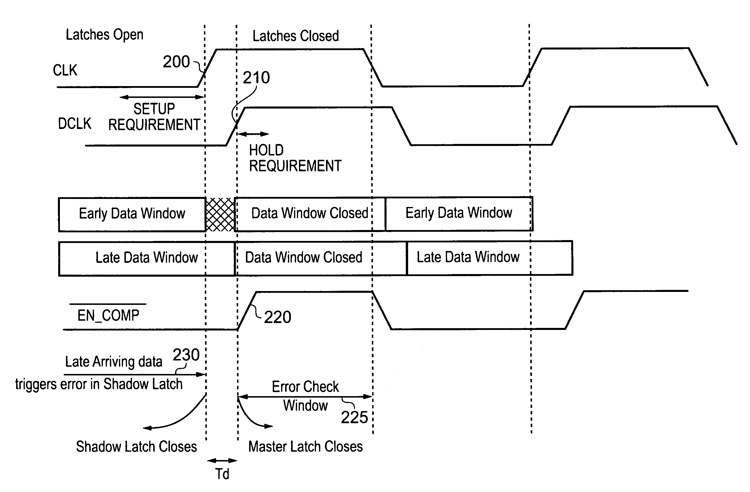
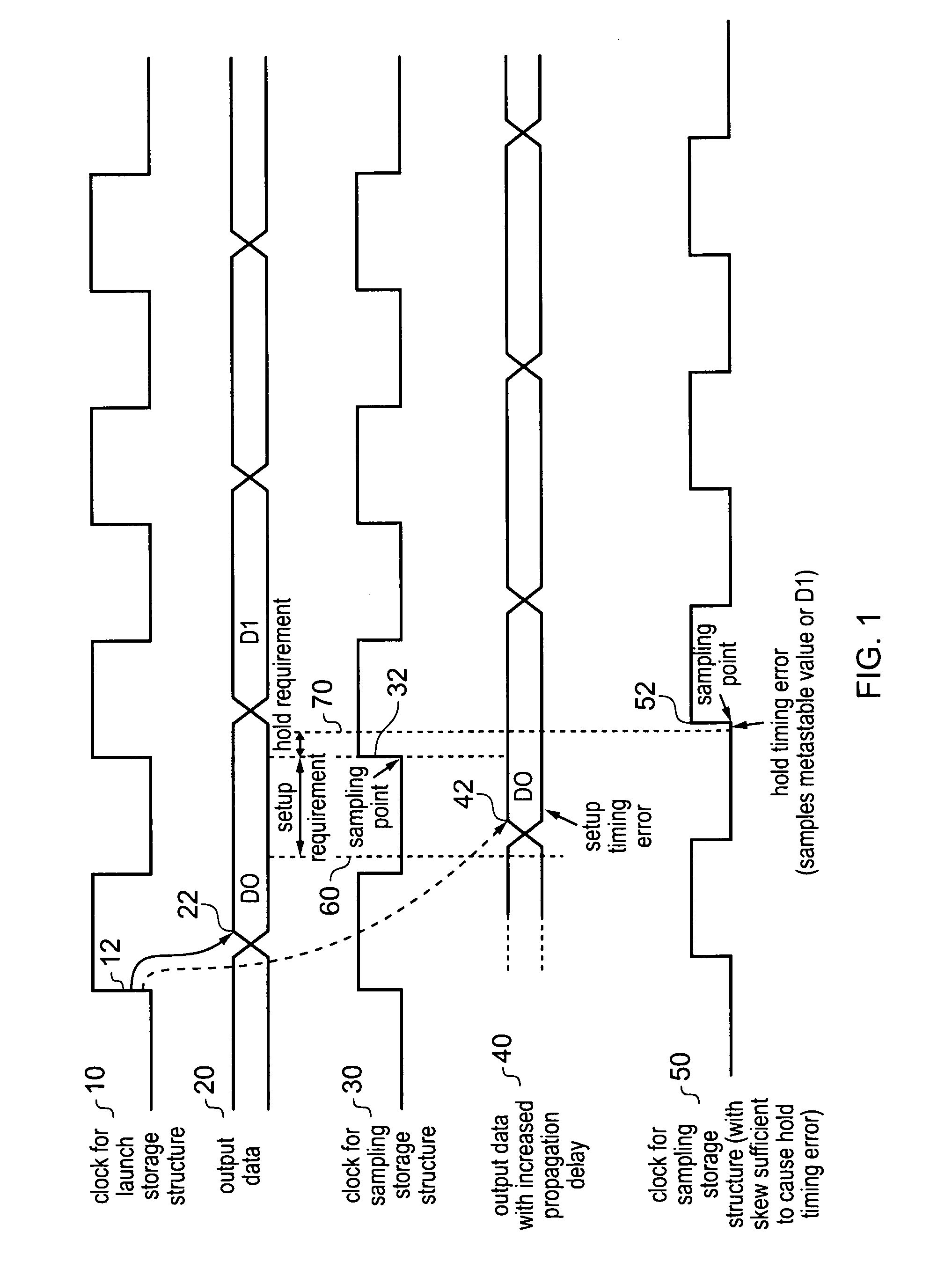
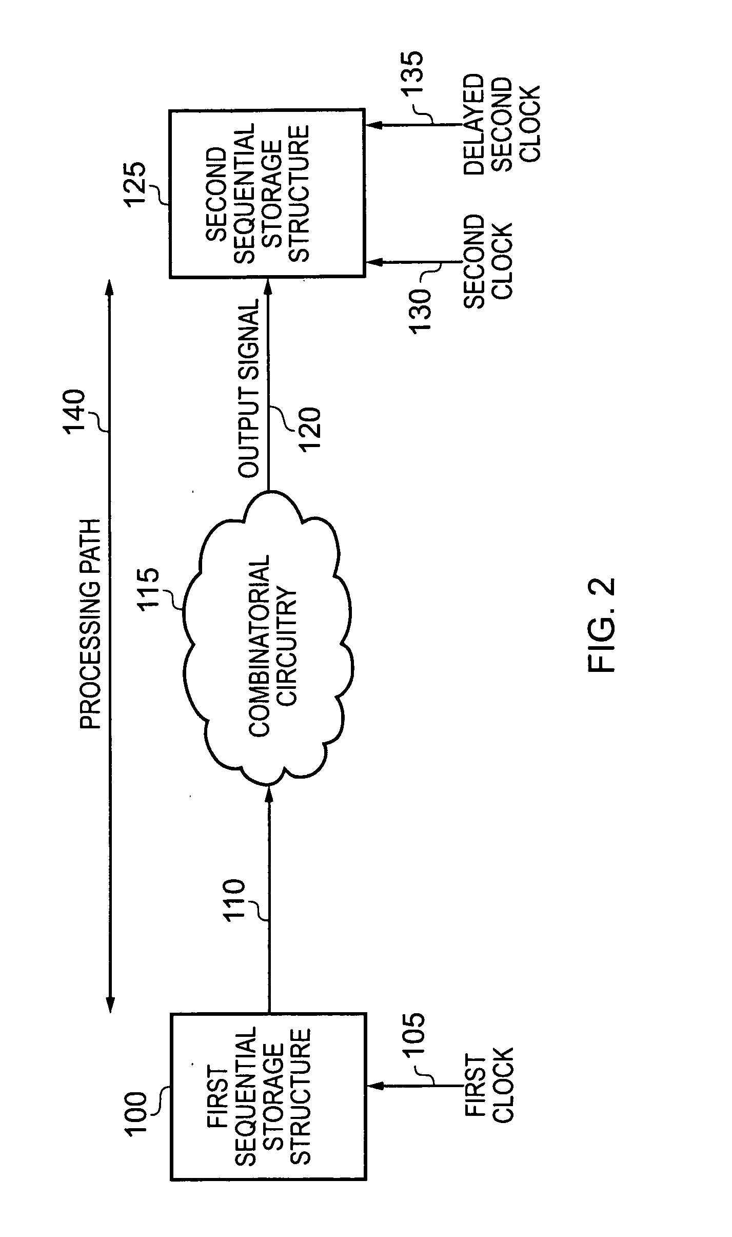
[0084]In the example shown in FIG. 7, it is assumed that the circuitry 300 can have its supply voltage dynamically varied via the intelligent energy management (IEM) / voltage scaling circuit 340. When the voltage scaling circuit 340 reduces the supply voltage, this can give rise to an increase in the propagation delay through the combinatorial circuits 310, 325. Accordingly, if the second sequential storage structures 315, 330 are configured as in FIG. 3, they can detect situations where a reduction in the supply voltage is giving rise to an approaching setup error condition before any actual error in operation of the second sequential storage circuit takes place. In particular, at the time the approaching error condition is detected, the second sequential storage structures will still be outputting correct data to any downstream circuitry within the data processing circuit 300. When an error signal is generated, this can be routed to the voltage scaling circuit 340, and may for exam...

second embodiment

[0085]Alternatively, or in addition, one or more second sequential storage structures configured as in FIG. 5 can also be used within the system of FIG. 7, to detect approaching hold timing related errors that may occur as the supply voltage is scaled.

[0086]FIG. 8 shows another system level application for the sequential storage structures of FIGS. 3 and 5. Within such a system, certain instances of the sequential storage structure can be configured as in FIG. 3 for performance limit detection using the sequential storage structure in canary setup mode (the first mode of operation) whilst other instances of the sequential storage structure can be configured as in FIG. 5 for functionality failure detection using the sequential storage structure in canary hold mode (the second mode of operation). In both modes of operation, the shadow latch 170 fails timing ahead of the functional element (i.e. the master-slave flip flop 150, 160) so that the system can detect the approaching timing e...


PUM


Abstract

An apparatus and method are provided for detecting an approaching error condition within a data processing apparatus. The data processing apparatus includes a second sequential storage structure which is arranged to latch the output signal generated by combinatorial circuitry dependent on a second clock signal. The second sequential storage structure has a main storage element to latch a value of the output signal for provision to subsequent combinatorial circuitry, and transition detection circuitry for detecting a change of the value of the output signal latched by the main storage element during a predetermined timing window, said change indicating an approaching error condition whilst the value stored in the main storage element is still correct. The second sequential storage structure can be operated in either a first mode of operation or a second mode of operation. In the first mode of operation, the predetermined timing window is a timing window ahead of a time at which the main storage element latches said value of the output signal, to thereby enable an approaching setup timing error due to a propagation delay within the combinatorial circuitry to be detected. In the second mode of operation, the predetermined timing window is a timing window after the time at which the main storage element latches said value of the output signal such that an approaching hold timing error due to an increase in skew between the first and second clock signals is detected. Such a technique provides a simple and efficient mechanism for detecting a variety of approaching error conditions whilst the second sequence storage structure continues to operate correctly.

Description

BACKGROUND OF THE INVENTION[0001]1. Field of the Invention[0002]The present invention relates to a data processing apparatus and method for detecting an approaching error condition at a time before an actual error occurs within the data processing apparatus.[0003]2. Description of the Prior Art[0004]The scaling of the size of components within data processing systems has long been a source of dramatic performance gains. In particular, developments in CMOS technology have enabled ever smaller feature sizes to be realised, which has enabled smaller circuits to be built exhibiting increased performance. However, it is also then desirable to reduce the operating voltage of such circuits, so as reduce power consumption and also decrease operating temperatures. However, the reduction in voltage levels has not been able to match the rate of feature size scaling because of limits in threshold voltage scaling, leading to increasing operating temperatures and current densities.[0005]Further, ...

Claims


Application Information

Patent Timeline
IPC IPC(8): G06F11/07
CPCG01R31/3016
Inventor IDGUNJI, SACHIN SATISHDAS, SHIDHARTHABULL, DAVID MICHAELAITKEN, ROBERT CAMPBELL
Owner ARM LTD
Why Eureka
Try Eureka