

Power semiconductor device
a technology of power semiconductor and semiconductor device, which is applied in the direction of semiconductor device, semiconductor/solid-state device details, electrical apparatus, etc., can solve the problems of transistor damage, and achieve the effect of suppressing damage to the power semiconductor device, preventing breakage of the power semiconductor device due to current concentration, and reducing the risk of electrical shock
- Summary
- Abstract
- Description
- Claims
- Application Information
AI Technical Summary
Benefits of technology
Problems solved by technology
Method used
Image

Examples
embodiment 1
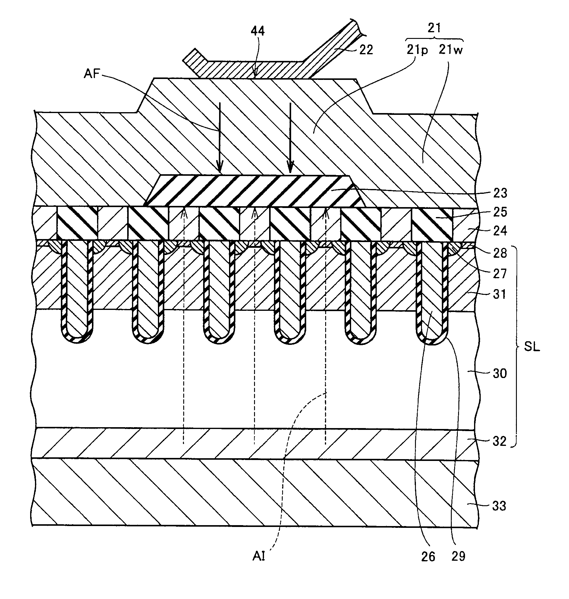
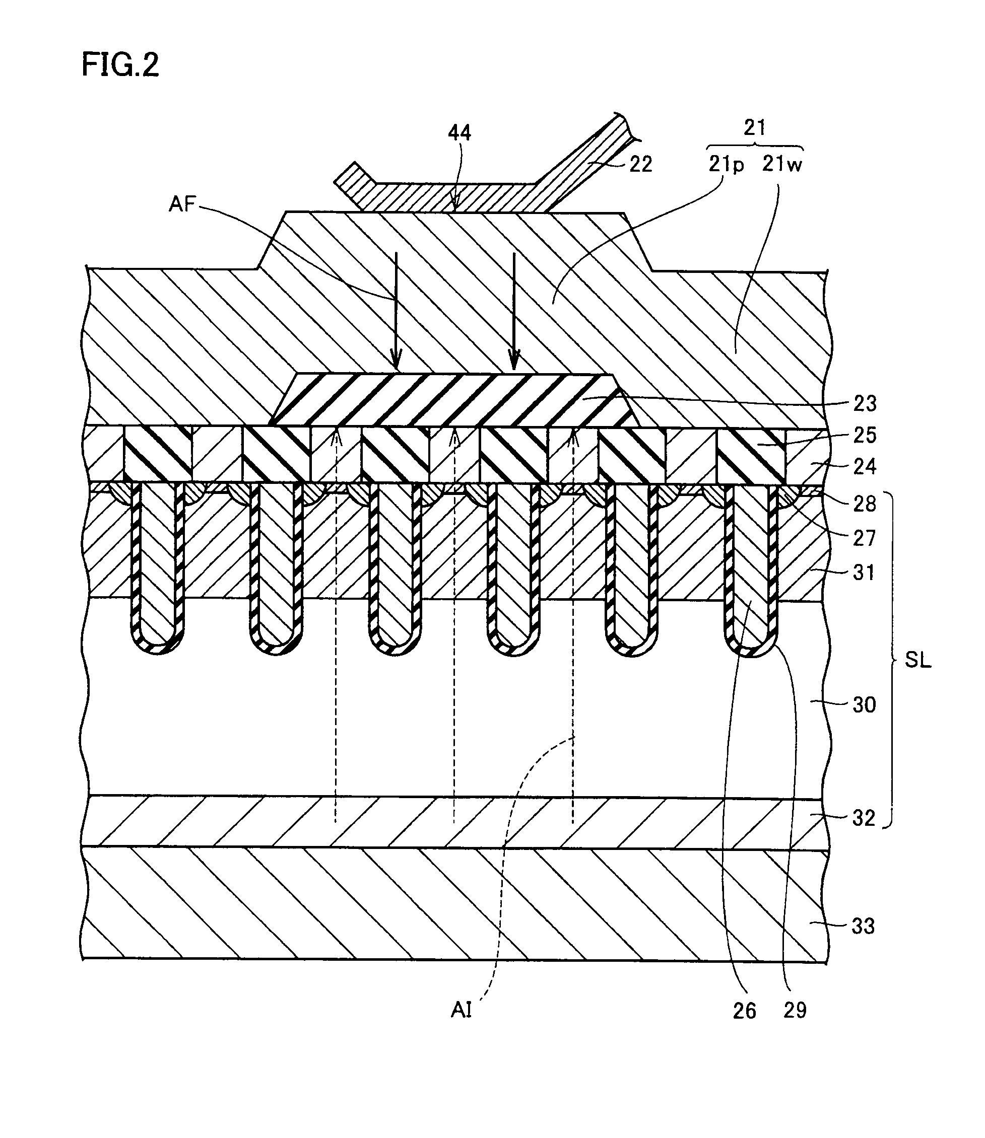
[0018]Referring to FIGS. 1 and 2, an IGBT as a power semiconductor device in accordance with the present embodiment has a semiconductor layer SL, a gate electrode 26, a gate insulating film 29, a conductor portion 24, an interlayer insulating film 25, a buffer insulating film 23, an emitter electrode 21 (electrode layer), a collector electrode 33, and a wire 22.
[0019]As a semiconductor portion of the IGBT, semiconductor layer SL has an nE layer 27 which will serve as an emitter, a p+ layer 28 for obtaining ohmic contact, an nB layer 30 called as a base or the like, and a pC layer 32 which will serve as a collector. nE layer 27 and nB layer 30 are n-type semiconductor layers, p+ layer 28, pB layer 31, and pc layer 32 are p-type semiconductor layers, and the semiconductor layers are silicon layers. Further, semiconductor layer SL has a plurality of trenches extending along one direction (i.e., a vertical direction in FIG. 1) and arranged to be spaced from one another in a direction in...
embodiment 2
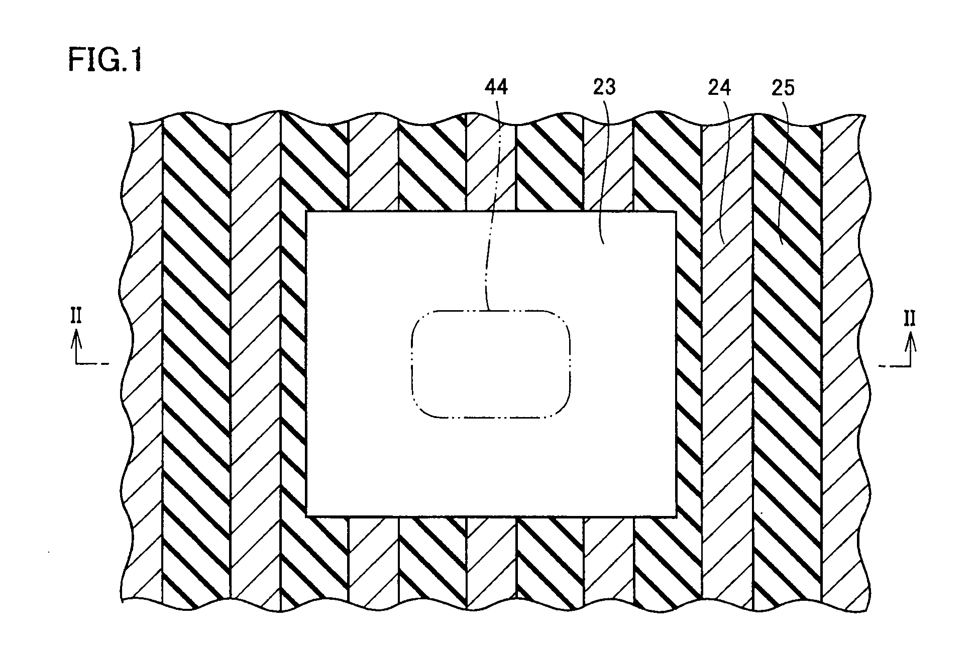
[0042]Referring to FIG. 4, a power semiconductor device in accordance with the present embodiment has a buffer insulating film 23V instead of buffer insulating film 23 (Embodiment 1: FIG. 1) Preferably, buffer insulating film 23V has an area that is not more than half the area of emitter electrode 21 (not shown in FIG. 4), as with buffer insulating film 23.
[0043]On buffer insulating film 23V, emitter electrode 21 covering buffer insulating film 23V is provided as in Embodiment 1. A portion of emitter electrode 21 on buffer insulating film 23V is a pad portion, and wire 22 (not shown in FIG. 4) is connected at each of a plurality of connection portions 44a, 44b.
[0044]Since the components other than that described above are substantially identical to those in Embodiment 1 described above, identical or corresponding elements will be designated by the same reference numerals, and the description thereof will not be repeated.
[0045]According to the present embodiment, a pad portion for a...
PUM
 Abstract
Description
Claims
Application Information