Antenna device and communication terminal apparatus

a technology of communication terminal and antenna device, which is applied in the direction of waveguide type devices, resonant antennas, inductances, etc., can solve the problems of insufficient gain, high cost, and high cost, and achieve the effect of preventing impedance change in the antenna device, reducing the and reducing the resultant or total inductance of the antenna elemen

Active Publication Date: 2011-12-22
MURATA MFG CO LTD
View PDF9 Cites 43 Cited by
  • Summary
  • Abstract
  • Description
  • Claims
  • Application Information

AI Technical Summary

Benefits of technology

[0021]According to the antenna device of various preferred embodiments of the present invention, since the impedance converting circuit generates an equivalent negative inductance that suppresses an effective inductance of the antenna element, a resulting or total inductance of the antenna element is reduced. As a result, the impedance frequency characteristic of the antenna device becomes small. Accordingly, it is possible to prevent impedance changes in the antenna device over a wide band and it is possible to achieve impedance matching with a power-supply circuit over a wide frequency band.

Problems solved by technology

However, since each of the matching circuits disclosed in Japanese Unexamined Patent Application Publication No. 2004-336250 and Japanese Unexamined Patent Application Publication No. 2006-173697 includes multiple resonant circuits, the insertion loss in the matching circuit is likely to increase and there are cases in which a sufficient gain is not obtained.
On the other hand, since the tunable antennas disclosed in Japanese Unexamined Patent Application Publication No. 2000-124728 and Japanese Unexamined Patent Application Publication No. 2008-035065 require a circuit for controlling a variable capacitance element, that is, a switching circuit for switching the frequency band, the circuit configuration is likely to be complicated.
Also, since loss and distortion in the switching circuit are large, there are cases in which a sufficient gain is not obtained.

Method used


Image

  • Antenna device and communication terminal apparatus
  • Antenna device and communication terminal apparatus
  • Antenna device and communication terminal apparatus

Examples


first preferred embodiment

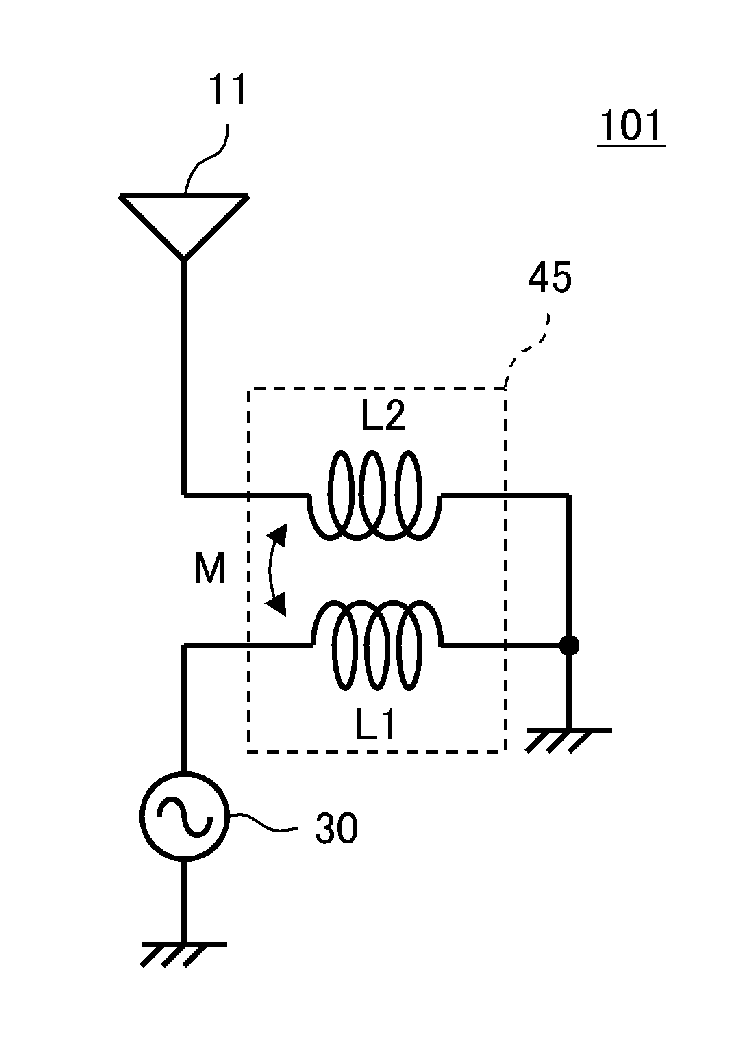
[0055]FIG. 1A is a circuit diagram of an antenna device 101 of a first preferred embodiment and FIG. 1B is an equivalent circuit diagram thereof.

[0056]As shown in FIG. 1A, the antenna device 101 includes an antenna element 11 and an impedance converting circuit 45 connected to the antenna element 11. The antenna element 11 preferably is a monopole antenna, for example. The impedance converting circuit 45 is connected to a power-supply end of the antenna element 11. The impedance converting circuit 45 is interposed between the antenna element 11 and a power-supply circuit 30. The power-supply circuit 30 preferably is a power-supply circuit that supplies high-frequency signals to the antenna element 11, and generates or processes the high-frequency signals. The power-supply circuit 30 may also include a circuit that combines or separates the high-frequency signals.

[0057]The impedance converting circuit 45 includes a first inductance element L1 connected to the power-supply circuit 30 ...

second preferred embodiment

[0068]FIG. 3A is a circuit diagram of an antenna device 102 of a second preferred embodiment and FIG. 3B is a diagram showing a specific arrangement of coil elements therein.

[0069]Although the basic configuration of the second preferred embodiment preferably is similar to the configuration of the first preferred embodiment, FIGS. 3A and 3B show a more specific configuration to cause a first inductance element and a second inductance element to couple to each other with a significantly high degree of coupling (i.e., to couple tightly as in transformer coupling).

[0070]As shown in FIG. 3A, a first inductance element L1 includes a first coil element L1a and a second coil element L1b, which are interconnected in series and are wound so as to define a closed magnetic path. A second inductance element L2 includes a third coil element L2a and a fourth coil element L2b, which are interconnected in series and are wound so as to define a closed magnetic path. In other words, the first coil ele...

third preferred embodiment

[0082]FIG. 6A is a perspective view of an impedance converting circuit 35 of a third preferred embodiment and FIG. 6B is a perspective view when the impedance converting circuit 35 is viewed from the lower-surface side. FIG. 7 is an exploded perspective view of a laminate 40 that provides the impedance converting circuit 35.

[0083]As shown in FIG. 7, a conductor pattern 61 is provided at a base layer 51a, which is an uppermost layer of the laminate 40, a conductor pattern 62 (62a and 62b) is provided at a base layer 51b, which is a second layer, and conductor patterns 63 and 64 are provided at a base layer 51c, which is a third layer. Two conductor patterns 65 and 66 are provided at a base layer 51d, which is a fourth layer, and a conductor pattern 67 (67a and 67b) is provided at a base layer 51e, which is a fifth layer. In addition, a ground conductor 68 is provided at a base layer 51f, which is a sixth layer, and a power-supply terminal 41, a ground terminal 42, and an antenna term...


PUM


Abstract

An antenna device includes an antenna element and an impedance converting circuit connected to the antenna element. The impedance converting circuit is connected to a power-supply end of the antenna element. The impedance converting circuit is interposed between the antenna element and a power-supply circuit. The impedance converting circuit includes a first inductance element connected to the power-supply circuit and a second inductance element coupled to the first inductance element. A first end and a second end of the first inductance element are connected to the power-supply circuit and the antenna, respectively. A first end and a second end of the second inductance element are connected to the antenna element and ground, respectively.

Description

BACKGROUND OF THE INVENTION[0001]1. Field of the Invention[0002]The present invention relates to an antenna device and a communication terminal apparatus including the same and particularly to an antenna device that achieves matching in a wide frequency band.[0003]2. Description of the Related Art[0004]In recent years, communication terminal apparatuses, such as portable phones, may require compatibility with communication systems, such as a GSM (Global System for Mobile Communication), DCS (Digital Communication System), PCS (Personal Communication Services), and UMTS (Universal Mobile Telecommunications System), as well as a GPS (Global Positioning System), a wireless LAN, Bluetooth (registered trademark), and so on. Thus, antenna devices for such communication terminal apparatuses are required to cover a wide frequency band of 800 MHz to 2.4 GHz.[0005]The antenna devices for a wide frequency band typically have a wideband matching circuit including an LC parallel resonant circuit...

Claims


Application Information

Patent Timeline
Patent Type & Authority Applications(United States)
IPC IPC(8): H01Q1/50H01P1/00H01P5/10H04B1/3822H04B1/40
CPCH01F17/0013H01P1/20345H01Q5/364H01Q9/30H01Q5/335H01P1/2135H01P5/08H01Q1/24H01Q1/50H01Q13/08
Inventor KATO, NOBORUISHIZUKA, KENICHI
Owner MURATA MFG CO LTD
Why Eureka
Try Eureka