Electrostatic discharge protection circuit

Inactive Publication Date: 2011-12-22
EMEMORY TECH INC
View PDF4 Cites 9 Cited by
  • Summary
  • Abstract
  • Description
  • Claims
  • Application Information

AI Technical Summary

Benefits of technology

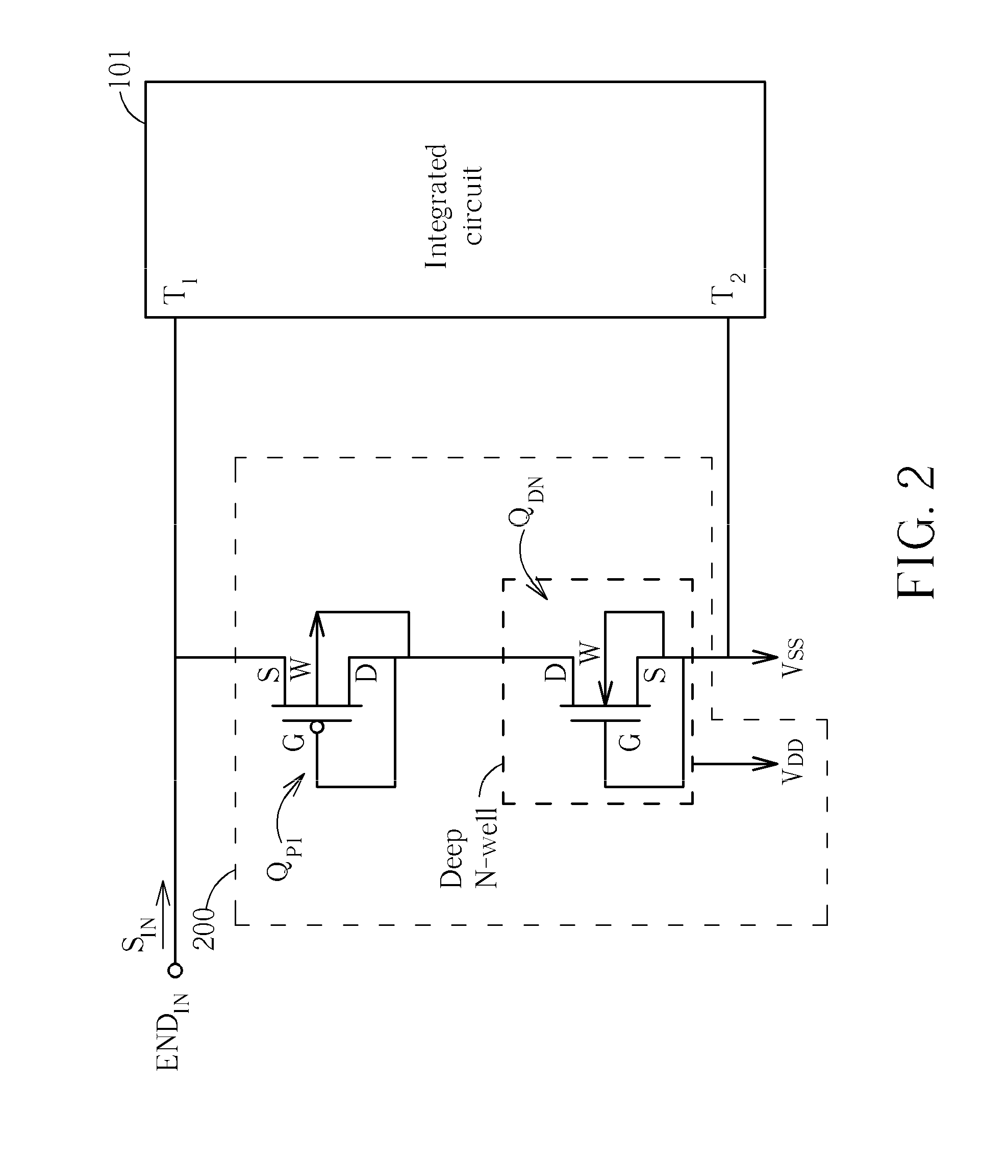
[0006]The present invention provides an electrostatic discharge (ESD) protection circuit. The ESD protection circuit is coupled between a first terminal and a second terminal of an integrated circuit for preventing the integrated circuit from being damaged by static electricity. The ESD protection circuit comprises a first P-channel Metal Oxide Semiconductor (PMOS) transistor and a deep N-well N-channel Metal Oxide Semiconductor (NMOS) transistor. The first PMOS transistor comprises a source, a drain, a gate, and an N-well. The source of the first PMOS transistor is coupled to the first terminal. The gate of the first PMOS transistor is coupled to the drain of the first PMOS transistor. The N-well of the first PMOS transistor is coupled to the drain of the first PMOS transistor. The deep N-well NMOS transistor comprises a source, a drain, a gate, a P-well, and a deep N-well. The source of the deep N-well NMOS transistor is coupled to the second terminal. The drain of the deep N-well NMOS transistor is coupled to the drain of the first PMOS transistor. The gate of the deep N-well NMOS transistor is coupled to the second terminal. The P-well of the deep N-well NMOS transistor is coupled to the source of the deep N-well NMOS transistor. The deep N-well of the deep N-well NMOS transistor is utilized for covering the P-well of the deep N-well NMOS transistor. The deep N-well of the deep N-well NMOS transistor is coupled to a second voltage source.

Problems solved by technology

In addition, when the voltage level of the input signal SIN is not within the operation voltage range, the leakage current is generated.

Method used


Image

  • Electrostatic discharge protection circuit
  • Electrostatic discharge protection circuit
  • Electrostatic discharge protection circuit

Examples


first embodiment

[0018]Please refer to FIG. 2 and FIG. 3. FIG. 2 is a diagram illustrating an ESD protection circuit 200 according to the present invention. FIG. 3 is a cross section diagram of the ESD protection circuit 200. In FIG. 3, N+ represents n-type doping, and P+ represents p-type doping. In FIG. 2, the ESD protection circuit 200 is coupled between the terminals T1 and T2 of the integrated circuit 101 for preventing the integrated circuit 101 from being damaged by the static electricity. The terminal T1 is utilized for the integrated circuit 101 to receive the input signal SIN and the terminal T2 is coupled to the voltage source VSS. The ESD protection circuit 200 includes a PMOS transistor QP1, and a deep N-well NMOS transistor QDN. The PMOS transistor QP1 includes a drain (D), a gate (G), a source (S), and an N-well (W), wherein the source of the PMOS transistor QP1 is coupled to the terminal T1, and the gate, the drain, and the N-well of the PMOS transistor QP1 are all coupled to the dee...

fifth embodiment

[0022]Please refer to FIG. 11. FIG. 11 is a diagram illustrating an ESD protection circuit 1000 according to the present invention. Compared with the ESD protection circuit 200, the ESD protection circuit 1000 further includes a driving circuit 1010 coupled to the gate of the deep N-well NMOS transistor QDN. The driving circuit 1010 includes a capacitor C and a resistor R. The first end of the capacitor C is coupled to the terminal T1. The second end of the capacitor C is coupled to the gate of the deep N-well NMOS transistor QDN. The first end of the resistor R is coupled to the gate of the deep N-well NMOS transistor QDN. The second end of the resistor R is coupled to the terminal T2. When the positive static electricity +ESD is generated from the input end ENDIN, since the static electricity has a high frequency, the gate of the deep N-well NMOS transistor QDN receives a high-level voltage through the capacitor C. In this way, the deep N-well NMOS transistor QDN is turned on, so ...

sixth embodiment

[0023]Please refer to FIG. 12. FIG. 12 is an ESD protection circuit 1100 according to the present invention. Compared with the ESD protection circuit 200, the ESD protection circuit 1100 further includes a driving circuit 1110 coupled to the gate of the deep N-well NMOS transistor QDN. The driving circuit 1110 includes an inverter INV, a capacitor C, and resistor R. The inverter INV includes a PMOS transistor QPINV, and an NMOS transistor QNINV. The well of the PMOS transistor QPINV is coupled to the source of the PMOS transistor QPINV, and the source of the PMOS transistor QPINV is coupled to the terminal T1. The drain of the PMOS transistor QPINV is coupled to the gate of the deep N-well NMOS transistor QDN. The well of the NMOS transistor QNINV is coupled to the source of the NMOS transistor QNINV, and the source of the NMOS transistor QNINV is coupled to the terminal T2. The drain of the NMOS transistor QNINV is coupled to the gate of the deep N-well NMOS transistor QDN. The fir...


PUM


Abstract

An electrostatic discharge (ESD) protection circuit is coupled between a first terminal and a second terminal of an integrated circuit. The integrated circuit receives an input signal through the first terminal. The second terminal is coupled to a voltage source. The ESD protection circuit includes a PMOS transistor and a deep N-well NMOS transistor. When the static electricity is inputted to the first terminal, the static electricity flows to the voltage source through the corresponding parasitic diode and the corresponding parasitic bipolar transistor of the PMOS transistor and the deep N-well NMOS transistor. In addition, the input signal is not affected by the ESD protection circuit because the parasitic diodes of the PMOS transistor and the deep N-well NMOS transistor are reversely connected. Thus, the ESD protection circuit prevents the integrated circuit from being damaged by the static electricity and increases the operation voltage range of the input signal.

Description

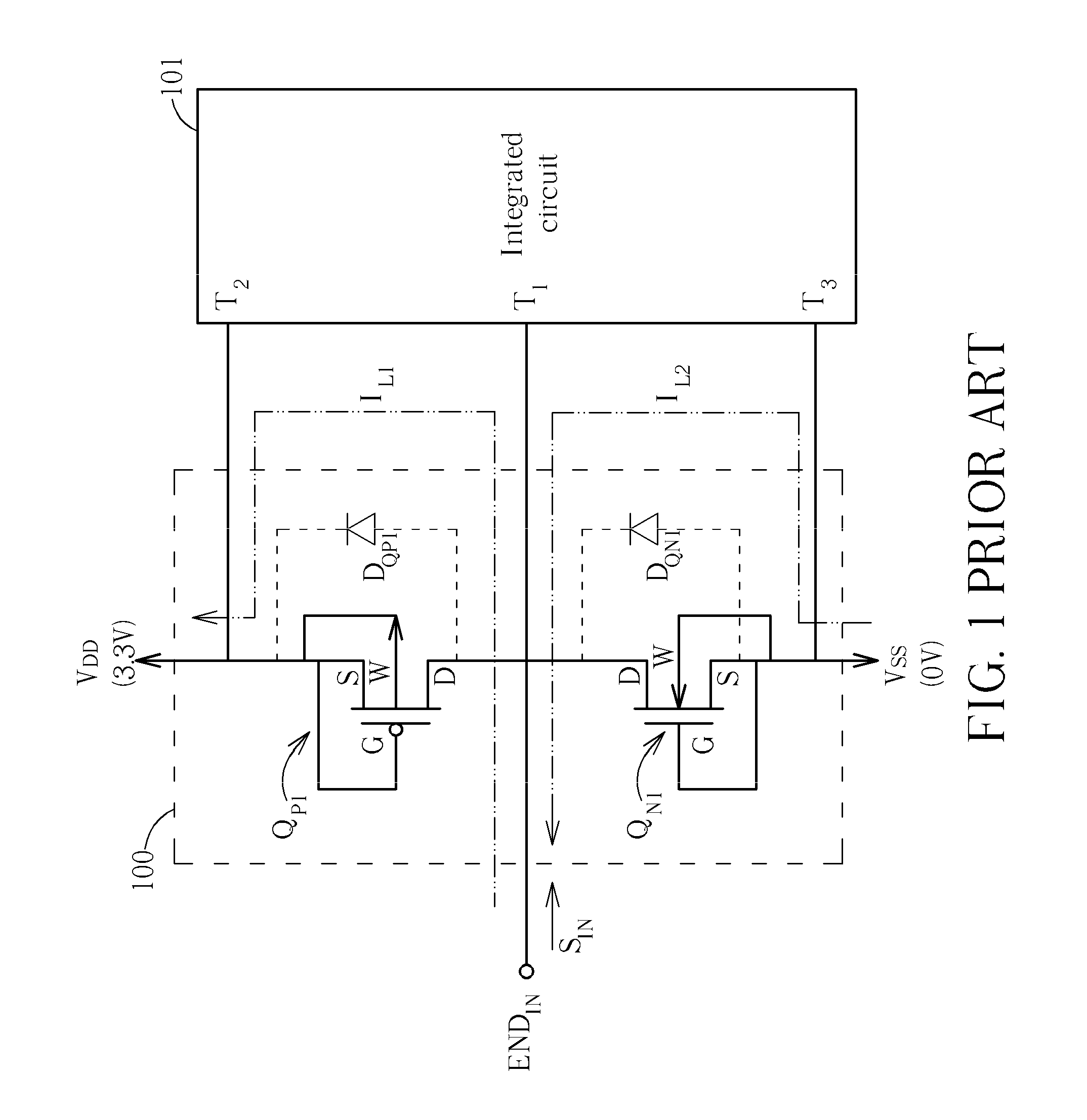
BACKGROUND OF THE INVENTION[0001]1. Field of the Invention[0002]The present invention is related to an electrostatic discharge (ESD) protection circuit for increasing the operation voltage range of a signal inputted into an integrated circuit.[0003]2. Description of the Prior Art[0004]Please refer to FIG. 1. FIG. 1 is a diagram illustrating a conventional ESD protection circuit 100. The ESD protection circuit 100 is coupled to terminals T1, T2, and T3 of an integrated circuit 101 for preventing the integrated circuit 101 from being damaged by the static electricity. The integrated circuit 101 receives an input signal SIN through the terminal T1; the terminal T2 is coupled to a voltage source VDD (for example, 3.3V); and the terminal T3 is coupled to a voltage source VSS (for example, 0V). The ESD protection circuit 100 includes a P-channel Metal Oxide Semiconductor (PMOS) transistor QP1 and an N-channel Metal Oxide Semiconductor (NMOS) transistor QN1. The PMOS transistor QP1 include...

Claims


Application Information

Patent Timeline
IPC IPC(8): H02H9/04H01L27/06
CPCH01L27/027
InventorHUANG, SHAO-CHANGLIN, WEI-YAOLEE, TANG-LUNGCHANG, KUN-WEISHEN, CHIUN-CHI
OwnerEMEMORY TECH INC