Light-Emitting Element, Light-Emitting Device, Display, and Electronic Device

a technology of light-emitting devices and light-emitting elements, which is applied in the direction of thermoelectric devices, organic semiconductor devices, other domestic articles, etc., can solve the problems of large pixel size, easy crosstalk, interference phenomenon between adjacent pixels, etc., and achieves high luminance. , the effect of great increase in driving voltag

Inactive Publication Date: 2011-12-29
SEMICON ENERGY LAB CO LTD
View PDF3 Cites 52 Cited by
  • Summary
  • Abstract
  • Description
  • Claims
  • Application Information

AI Technical Summary

Benefits of technology

[0009]In the light-emitting element disclosed in Patent Document 1, in which EL layers are stacked and separated from each other by a charge generation layer, an electron injection buffer layer is provided together with the charge generation layer as an intermediate layer in many cases in order to easily inject electrons generated in the charge generation layer to the EL layer and to reduce driving voltage. In particular, when a high-definition monochrome display or a high-definition display achieving full color display using a color filter or a color conversion layer is manufactured using such a light-emitting element, there is a problem in that crosstalk easily occurs because a plurality of light-emitting elements shares one intermediate layer.
[0041]Furthermore, according to one embodiment of the present invention, a light-emitting device with high display quality can be provided. A display with high display quality can be provided. An electronic device including a display portion with high display quality can be provided.

Problems solved by technology

In the case of manufacturing a high-definition display, problems which do not occur in lighting application and a display having a large pixel size are caused in some cases.
One of such problems is an interference phenomenon between adjacent pixels, that is, crosstalk.
In particular, when a high-definition monochrome display or a high-definition display achieving full color display using a color filter or a color conversion layer is manufactured using such a light-emitting element, there is a problem in that crosstalk easily occurs because a plurality of light-emitting elements shares one intermediate layer.

Method used


Image

  • Light-Emitting Element, Light-Emitting Device, Display, and Electronic Device
  • Light-Emitting Element, Light-Emitting Device, Display, and Electronic Device
  • Light-Emitting Element, Light-Emitting Device, Display, and Electronic Device

Examples


embodiment 1

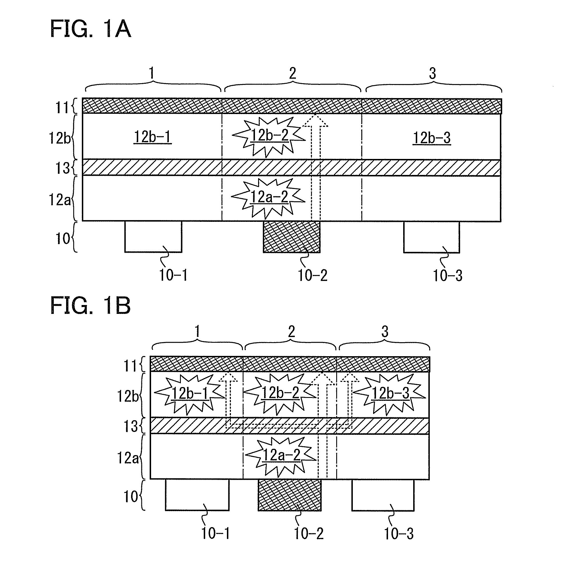
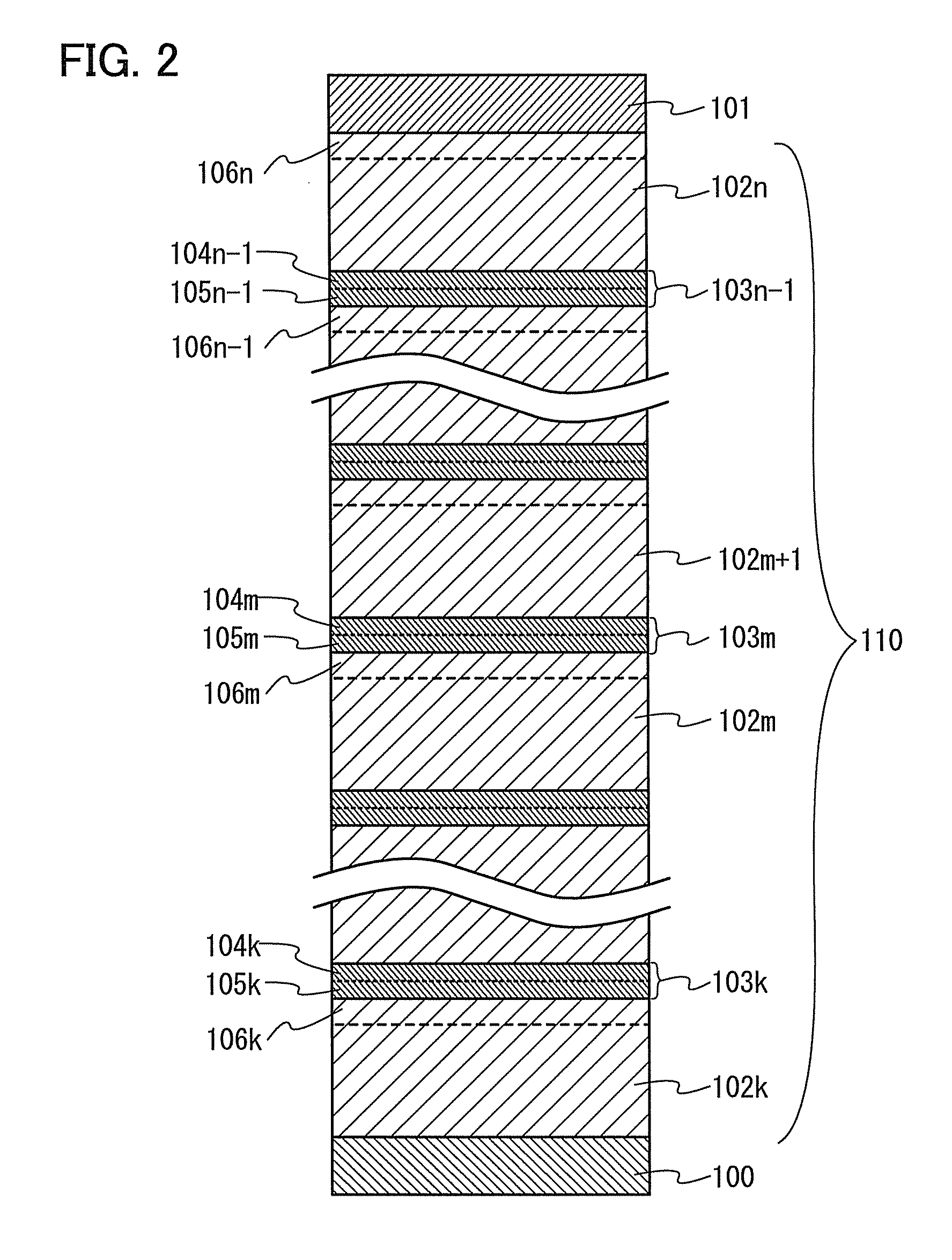
[0066]A conceptual diagram of a light-emitting element according to one embodiment of the present invention is illustrated in FIG. 2. The light-emitting element illustrated in FIG. 2 includes n EL layers between a pair of electrodes (an anode 100 and a cathode 101). The EL layer which is the closest to the anode 100 is referred to as a first EL layer 102k, and the EL layer which is the closest to the cathode 101 is referred to as an n-th EL layer 102n. The light-emitting element illustrated in FIG. 2 includes the EL layers (i.e., the first EL layer 102k . . . an nigh EL layer 102m . . . the n-th EL layer 102n); intermediate layers (i.e., a first intermediate layer 103k . . . an m-th intermediate layer 103m . . . a (n−1)-th intermediate layer 103n−1); first layers (i.e., a first first layer 104k . . . an m-th first layer 104m . . . a (n−1)-th first layer 104n−1); second layers (i.e., a first second layer 105k . . . an m-th second layer 105m . . . a (n−1)-th second layer 105n−1); elec...

embodiment 2

[0129]In this embodiment, an example of a light-emitting device which is manufactured using the light-emitting element described in Embodiment 1 will be described. Note that the light-emitting device in one embodiment of the present invention is not limited to a light-emitting device having a structure described below, and it includes, in its category, all modes in each of which a display portion (e.g., a pixel portion 602 in this embodiment) includes the light-emitting element described in Embodiment 1.

[0130]In this embodiment, an example of a light-emitting device manufactured using the light-emitting element described in Embodiment 1 will be described with reference to FIGS. 3A and 3B. Note that FIG. 3A is a top view illustrating the light-emitting device and FIG. 3B is a cross-sectional view taken along lines A-A′ and B-B′ in FIG. 3A. The light-emitting device includes a driver circuit portion (source line driver circuit) 601, a pixel portion 602, and a driver circuit portion (g...

embodiment 3

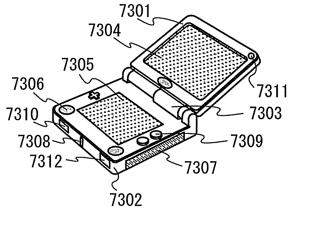
[0156]In this embodiment, examples of various electronic devices and lighting devices, which are completed using the light-emitting device of one embodiment of the present invention, such as described in Embodiment 2, will be described with reference to FIGS. 7A to 7D.

[0157]Examples of the electronic devices to which the light-emitting device is applied include television devices (also referred to as televisions or television receivers), monitors of computers or the like, cameras such as digital cameras or digital video cameras, digital photo frames, cellular phones (also referred to as mobile phones or cellular phone devices), portable game machines, portable information terminals, audio reproducing devices, large-sized game machines such as pachinko machines, and the like. Specific examples of these electronic devices are described below.

[0158]FIG. 7A illustrates an example of a television device. In the television device, a display portion 7103 is incorporated in a housing 7101. ...


PUM


Abstract

In the light-emitting element in which a plurality of EL layers is separated from each other by a charge generation layer, provided are an electron relay layer in contact with an anode side of the charge generation region and an electron transport layer in contact with the electron relay layer. The electron transport layer contains an alkaline earth metal. A concentration gradient of the alkaline earth metal contained in the electron transport layer is such that the concentration of the alkaline earth metal becomes lower from an interface between the electron transport layer and the electron relay layer to the anode.

Description

TECHNICAL FIELD[0001]The present invention relates to a light-emitting element which includes a light-emitting layer containing an organic compound between a pair of electrodes. Further, the present invention relates to a light-emitting device including the light-emitting element and an electronic device including the light-emitting device.BACKGROUND ART[0002]In recent years, mobile devices show remarkable development, and one can easily enjoy image works anytime and anywhere with a small image reproducing device, a display attached to a mobile phone, and the like. Further, image data is being more often downloaded or transferred by a small memory, and the demand for the mobile devices is expected to increase.[0003]In order to enjoy high-quality image works with a small display such as a display attached to a mobile phone, the display is required to have sufficiently high definition.[0004]Meanwhile, a light-emitting element (also referred to as an electroluminescence element or an E...

Claims


Application Information

Patent Timeline
Patent Type & Authority Applications(United States)
IPC IPC(8): H01L51/54
CPCH01L27/3244H01L51/0059H01L51/0072H01L51/0074H01L51/0078Y10S428/917H01L51/0085H01L51/5004H01L51/5052H01L51/5278H01L2251/5346H01L51/0081H10K59/12H10K85/631H10K85/311H10K85/6576H10K85/324H10K85/342H10K85/6572H10K50/11H10K2101/40H10K50/155H10K50/165H10K50/19H10K2101/80C09B47/04C07F1/08H10K50/00
Inventor NOWATARI, HIROMISEO, SATOSHIOHSAWA, NOBUHARU
Owner SEMICON ENERGY LAB CO LTD
Why Eureka
Try Eureka