Liquid crystal display and method of manufacturing liquid crystal display

a liquid crystal display and liquid crystal technology, applied in the field of liquid crystal display, can solve the problems of difficult to obtain high transmittance, difficult to align liquid crystal molecules, and difficult to achieve high transmittance, so as to achieve efficient pre-tilt, reduce the effect of transmittance suppression and high transmittan

Active Publication Date: 2011-12-29
SONY CORP
View PDF9 Cites 39 Cited by
  • Summary
  • Abstract
  • Description
  • Claims
  • Application Information

AI Technical Summary

Benefits of technology

[0013]In the liquid crystal display and the method of manufacturing the liquid crystal display according to the embodiments of the present invention, the concavo-convex structure is provided on one or both of the face on the liquid crystal layer side of the pixel electrode, and the face on the liquid crystal layer side of the opposite electrode. Thus, in the liquid crystal layer when a voltage is applied thereto, distortion of an electric field (lateral electric field) is generated due to height difference (step) between a concave face and a convex face in the concavo-convex structure. Meanwhile, there is no notched portion in the electrode, such as a slit, so a region to which the voltage is not applied in the liquid crystal layer is eliminated, and alignment of liquid crystal molecules is suppressed from being insufficient in a local region.
[0014

Problems solved by technology

However, in the above-described methods, it is possible to improve the voltage response characteristics, but the voltage is not applied to a portion corresponding to the slit in the liquid crystal layer (immediately above the slit), and it is difficult to align the

Method used


Image

  • Liquid crystal display and method of manufacturing liquid crystal display
  • Liquid crystal display and method of manufacturing liquid crystal display
  • Liquid crystal display and method of manufacturing liquid crystal display

Examples


modification 1

[0121]2. Modification 1

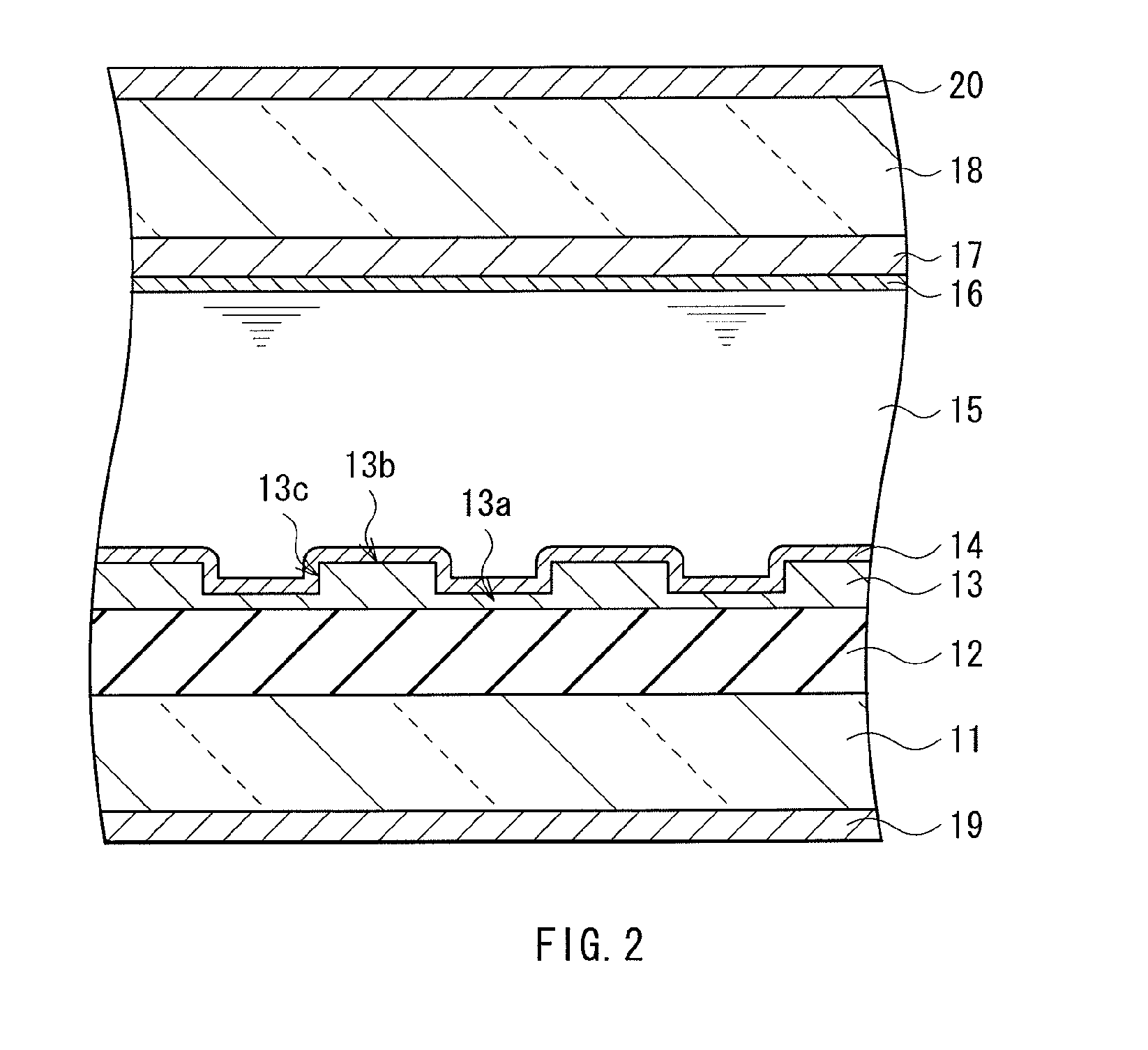
[0122]FIG. 17 illustrates the cross-sectional structure (corresponds to part of the pixel) of the liquid crystal display panel in the liquid crystal display according to Modification 1. Like the liquid crystal display panel 2 of the above-described embodiment, in the liquid crystal display panel of this modification, the liquid crystal layer 15 is sandwiched between the drive substrate 11 and the facing substrate 18, and the polarizing plates 19 and 20 are bonded onto the outer faces of the drive substrate 11 and the facing substrate 18, respectively. A planarizing film 21 is formed on the drive substrate 11 so as to cover the surface of the drive substrate 11, and a pixel electrode 22 is disposed for each pixel 10 on the planarizing film 21. In such a structure, in this modification, the face on the liquid crystal layer 15 side of the pixel electrode 22 has the concave-convex structure, and the face on the liquid crystal layer 15 side of the opposite electrod...

modification 2

[0126]3. Modification 2

[0127]FIGS. 19A to 19C illustrates another manufacturing method of the pixel electrode 13 in the liquid crystal display according to Modification 2 in a process order. In the above-described embodiment, after the pixel electrode 13 is formed over the whole surface of the planarizing film 12, the concavo-convex structure of the pixel electrode 13 is formed by half-etching, but it is also possible to form the concavo-convex structure as will be described next. That is, as illustrated in FIG. 19A, after the planarizing film 21 is formed on the drive substrate 11, an electrode layer 130 of ITO is formed over the whole surface of the planarizing film 21 by, for example, the evaporation method or the sputtering. Next, as illustrated in FIG. 19B, the selective region (the region corresponding to the concave face 13a) of the electrode layer 130 is, for example, removed by etching using the photolithography. After this, as illustrated in FIG. 19C, an electrode layer 13...

modification 3

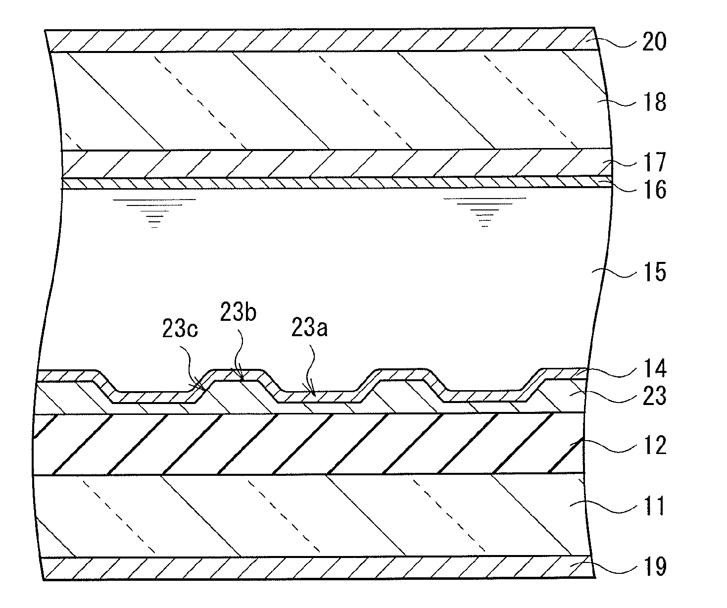
[0129]4. Modification 3

[0130]FIG. 20 illustrates the cross-sectional structure (corresponding to part of the pixel) of the liquid crystal display panel in the liquid crystal display according to Modification 3. Like the liquid crystal display panel 2 of the above-described embodiment, in the liquid crystal display panel of this modification, the liquid crystal layer 15 is sandwiched between the drive substrate 11 and the facing substrate 18, and the polarizing plates 19 and 20 are bonded the onto outer faces of the drive substrate 11 and the facing substrate 18, respectively. A pixel electrode 23 is disposed for each pixel 10 above the drive substrate 11 with the planarizing film 12 in between. In such a structure, also in this modification, the face on the liquid crystal layer 15 side of the pixel electrode 23 has the concave convex structure, and the face on the liquid crystal layer 15 side of the opposite electrode 17 is flat.

[0131]However, in this modification, the concavo-conve...


PUM


Abstract

A liquid crystal display capable of realizing a high transmittance while maintaining favorable voltage response characteristics, and a method of manufacturing the same are provided. The liquid crystal display includes: a liquid crystal layer; a first substrate and a second substrate arranged to face each other with the liquid crystal layer in between; a plurality of pixel electrodes provided on a liquid crystal layer side of the first substrate; and an opposite electrode provided on the second substrate to face the plurality of pixel electrodes. One or both of a face on the liquid crystal layer side of the pixel electrode, and a face on the liquid crystal layer side of the opposite electrode includes a concavo-convex structure.

Description

RELATED APPLICATION DATA[0001]This application claims priority to Japanese Priority Patent Application JP 2010-087658, filed in the Japan Patent Office on Apr. 6, 2010, and Japanese Priority Patent Application JP 2011-038640, filed in the Japan Patent Office on Feb. 24, 2011, the entire contents of both of which are hereby incorporated by reference to the extent permitted by law.BACKGROUND OF THE INVENTION[0002]1. Field of the Invention[0003]The present invention relates to a liquid crystal display using, for example, liquid crystal of a VA mode, and a method of manufacturing the same.[0004]2. Description of the Related Art[0005]In recent years, for example, a VA (vertical alignment) mode is used in liquid crystal display (LCD) devices. In the liquid crystal displays, a liquid crystal layer having the refractive index anisotropy is sealed between a substrate including a pixel electrode and a substrate including an opposite electrode, and a voltage is applied to the liquid crystal la...

Claims


Application Information

Patent Timeline
IPC IPC(8): G02F1/1335G02F1/1333H01L33/08G02F1/1343
CPCG02F1/133371G02F1/134309G02F1/133707G02F1/133788G02F1/1339G02F1/13439G02F1/133357
Inventor NAKAMURA, MASAHIKOSUWA, SHUNICHIMIYAKAWA, MASASHIINOUE, YUICHIISOZAKI, TADAAKINAGASE, YOJI
Owner SONY CORP
Why Eureka
Try Eureka