Liquid crystal display device

a liquid crystal display and active matrix technology, applied in the field of active matrix liquid crystal display devices, can solve the problems of color breakage and other problems, and achieve the effect of prolonging the time for holding a voltage applied to a liquid crystal elemen

Active Publication Date: 2012-01-05
SEMICON ENERGY LAB CO LTD +1
View PDF12 Cites 51 Cited by
  • Summary
  • Abstract
  • Description
  • Claims
  • Application Information

AI Technical Summary

Benefits of technology

[0029]In a liquid crystal display device according to an embodiment of the present invention, a pixel portion is divided into a plurality of regions, and lights whose hues are different from each other are sequentially supplied per region, whereby a color image is displayed. Therefore, at each time, a hue of a light supplied to a region can be different from a hue of a light supplied to the adjacent region. Consequently, separate perception of images for respective colors without synthesis can be prevented, so that a color break-up, which has been likely to occur in displaying a moving image, can be prevented from occurring.
[0030]According to an embodiment of the present invention, it is possible to realize a liquid crystal display device capable of image display using a reflective mode utilizing external light as a light source and a transmissive mode utilizing a backlight according to an environment around the liquid crystal display device, e.g., in a bright environment or a dim environment. For example, a moving image is displayed using a transmissive mode, and a still image is displayed using a reflective mode.
[0031]According to an embodiment of the present invention, a transistor whose off-state current is extremely low is used in the pixel portion, whereby a period for holding a voltage applied to a liquid crystal element can be prolonged. Therefore, the driving frequency for displaying a still image can be decreased to a frequency lower than the driving frequency for displaying a moving image. Consequently, a liquid crystal display device whose power consumption is low can be achieved.

Problems solved by technology

However, separate perception of images for respective colors without synthesizing them, a so-called color break-up is likely to occur in the FS driving.

Method used


Image

  • Liquid crystal display device
  • Liquid crystal display device
  • Liquid crystal display device

Examples


embodiment 1

Structure Example of Liquid Crystal Display Device

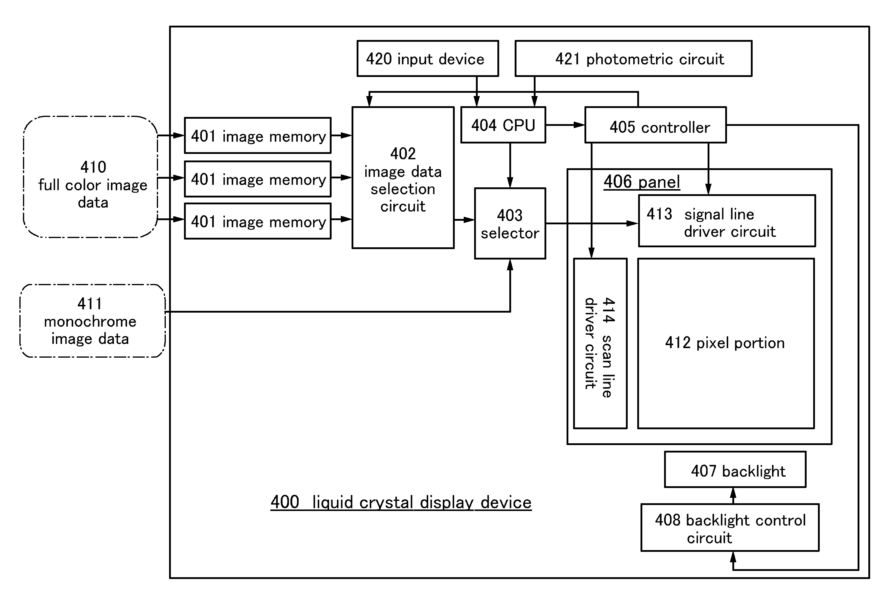
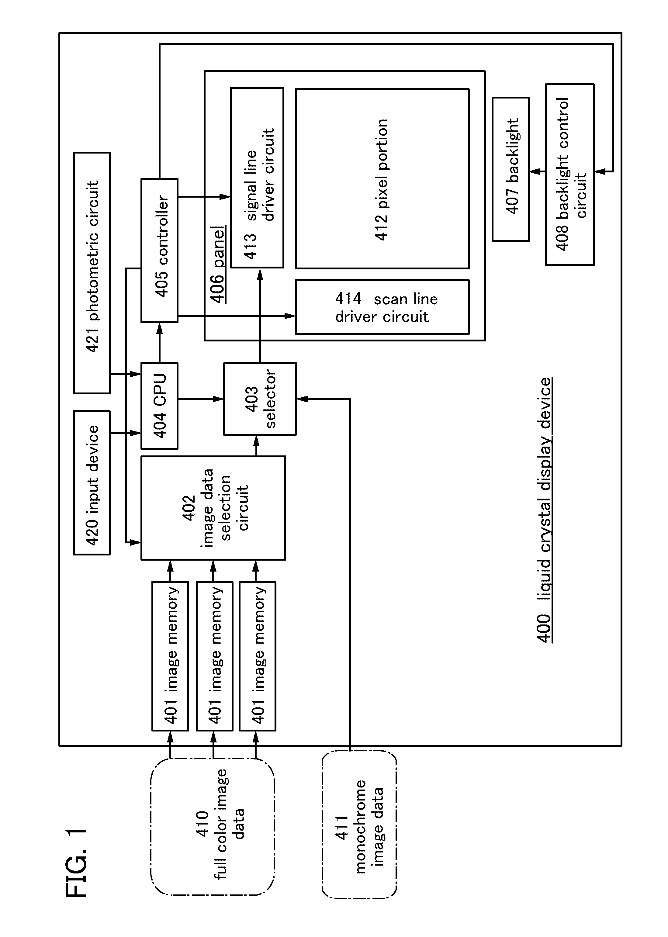
[0067]A liquid crystal display device 400 illustrated in FIG. 1 includes a plurality of image memories 401, an image data selection circuit 402, a selector 403, a CPU 404, a controller 405, a panel 406, a backlight 407, and a backlight control circuit 408.

[0068]Image data corresponding to a full-color image (full-color image data 410), which are input to the liquid crystal display device 400, are stored in the plurality of image memories 401. The full-color image data 410 include image data for their respective hues. The image data for the respective hues are stored in the respective image memories 401.

[0069]As the image memories 401, for example, memory circuits such as dynamic random access memories (DRAMs) or static random access memories (SRAMs) can be used.

[0070]The image data selection circuit 402 reads the full-color image data for the respective hues, which are stored in the plurality of image memories 401, and sends the full...

configuration example 1

of Pulse Output Circuit

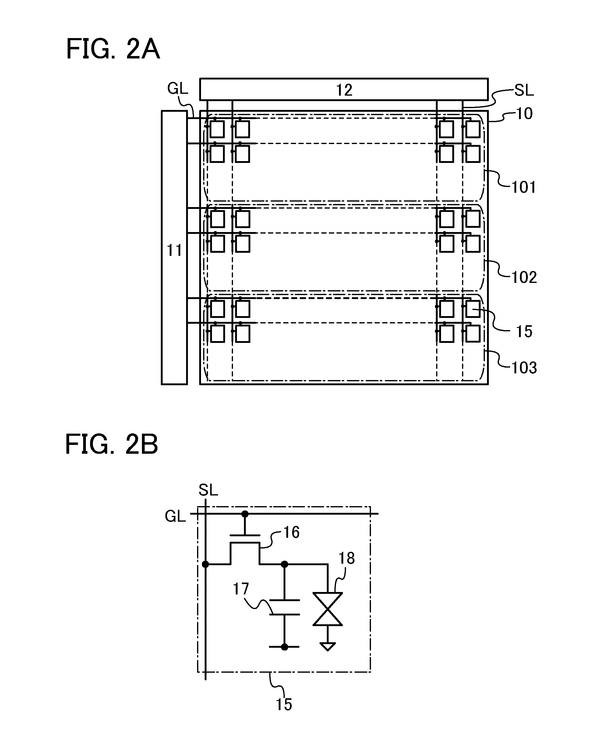
[0135]Next, FIG. 8A illustrates an example of a specific configuration of the x-th pulse output circuit 20—x illustrated in FIG. 7. The pulse output circuit illustrated in FIG. 8A includes transistors 31 to 39.

[0136]A gate electrode of the transistor 31 is connected to the terminal 21. A first terminal of the transistor 31 is connected to a node supplied with a high power supply potential (Vdd). A second terminal of the transistor 31 is connected to a gate electrode of the transistor 33 and a gate electrode of the transistor 38.

[0137]A gate electrode of the transistor 32 is connected to a gate electrode of the transistor 34 and a gate electrode of the transistor 39. A first terminal of the transistor 32 is connected to a node supplied with a low power supply potential (Vss). A second terminal of the transistor 32 is connected to the gate electrode of the transistor 33 and the gate electrode of the transistor 38.

[0138]A first terminal of the transistor 33 is co...

configuration example 2

of Pulse Output Circuit

[0208]FIG. 19A illustrates another example of the configuration of the pulse output circuit. The pulse output circuit illustrated in FIG. 19A includes a transistor 50 in addition to the configuration of the pulse output circuit illustrated in FIG. 8A. A first terminal of the transistor 50 is connected to the node supplied with the high power supply potential. A second terminal of the transistor 50 is connected to the gate electrode of the transistor 32, the gate electrode of the transistor 34, and the gate electrode of the transistor 39. A gate electrode of the transistor 50 is connected to a reset terminal (Reset).

[0209]A high-level potential is input to the reset terminal in a period which follows the round of switching of hues of the backlight in the pixel portion; a low-level potential is input in the other periods. Note that the transistor 50 is turned on by input of a high-level potential. Thus, the potential of each node can be initialized in the period...


PUM


Abstract

A liquid crystal display device comprising a backlight and a pixel portion including first to 2n-th scan lines, wherein, in a first case of expressing a color image, first pixels controlled by the first to n-th scan lines are configured to express a first image using at least one of first to third hues supplied in a first rotating order, and second pixels controlled by the (n+1)-th to 2n-th scan lines are configured to express a second image using at least one of the first to third hues supplied in a second rotating order, wherein, in a second case of expressing a monochrome image, the first and second pixels controlled by the first to 2n-th scan lines are configured to express the monochrome image by external light reflected by the reflective pixel electrode, and wherein the first rotating order is different from the second rotating order.

Description

BACKGROUND OF THE INVENTION[0001]1. Field of the Invention[0002]The present invention relates to an active-matrix liquid crystal display device including a transistor in a pixel.[0003]2. Description of the Related Art[0004]In a transmissive liquid crystal display device, power consumption of a backlight largely affects power consumption of the whole of the liquid crystal display device, and therefore, reduction of light loss inside a panel is important for reduction of power consumption. Light loss inside a panel is caused by light refraction in an interlayer insulating film, light absorption in a color filter, or the like. In particular, the light loss by a color filter is large in principle in the color filter in which light absorption by a pigment is used to extract light having a predetermined range of wavelengths from white light. As a matter of fact, 70% or more of the energy of light from the backlight is absorbed by the color filter. As described above, the color filter hind...

Claims


Application Information

Patent Timeline
Patent Type & Authority Applications(United States)
IPC IPC(8): G09G5/10G09G3/36
CPCG09G3/2025G09G3/3406G09G2330/021G09G2300/0456G09G3/3607G09G3/3413G09G3/3659
Inventor YAMAZAKI, SHUNPEIKOYAMA, JUNMIYAKE, HIROYUKITOYOTAKA, KOUHEI
Owner SEMICON ENERGY LAB CO LTD
Why Eureka
Try Eureka