Graphene processing for device and sensor applications

a technology of graphene and sensor, applied in the direction of instruments, transportation and packaging, coatings, etc., can solve the problems of difficult control of the number of graphene layers and grain sizes, limited to the tedious fabrication of devices for research purposes, and the difficulty inherent in the method of dispersing graphene in solution separation of layers without breaking layers

Inactive Publication Date: 2012-01-05
UNIV OF FLORIDA RES FOUNDATION INC
View PDF3 Cites 61 Cited by
  • Summary
  • Abstract
  • Description
  • Claims
  • Application Information

AI Technical Summary

Benefits of technology

This patent describes how to create a new type of material called supported graphene. By adding carbon to a substrate and then converting it to graphene through a process known as epitaxy, researchers have been able to produce this unique material. The method involves heating the substrate and the added carbon until they become compatible with each other, allowing for the growth of multiple layers of graphene. The resulting material could have various applications such as electronics, sensors, and optics.

Problems solved by technology

The technical problem addressed in this patent is finding ways to reliably and efficiently produce large amounts of pure graphene sheets, which remain expensive and difficult to obtain through current methods such as exfoliation. Existing methods require long periods of time and special equipment, making it hard to scale up production. If there were a more efficient way to make and isolate graphene sheets, they could become much more commercially viable.

Method used


Image

  • Graphene processing for device and sensor applications
  • Graphene processing for device and sensor applications

Examples


Embodiment Construction

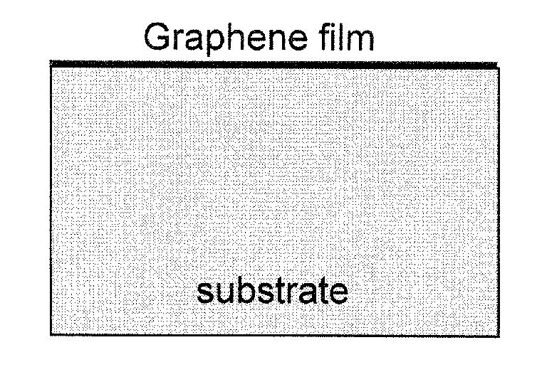
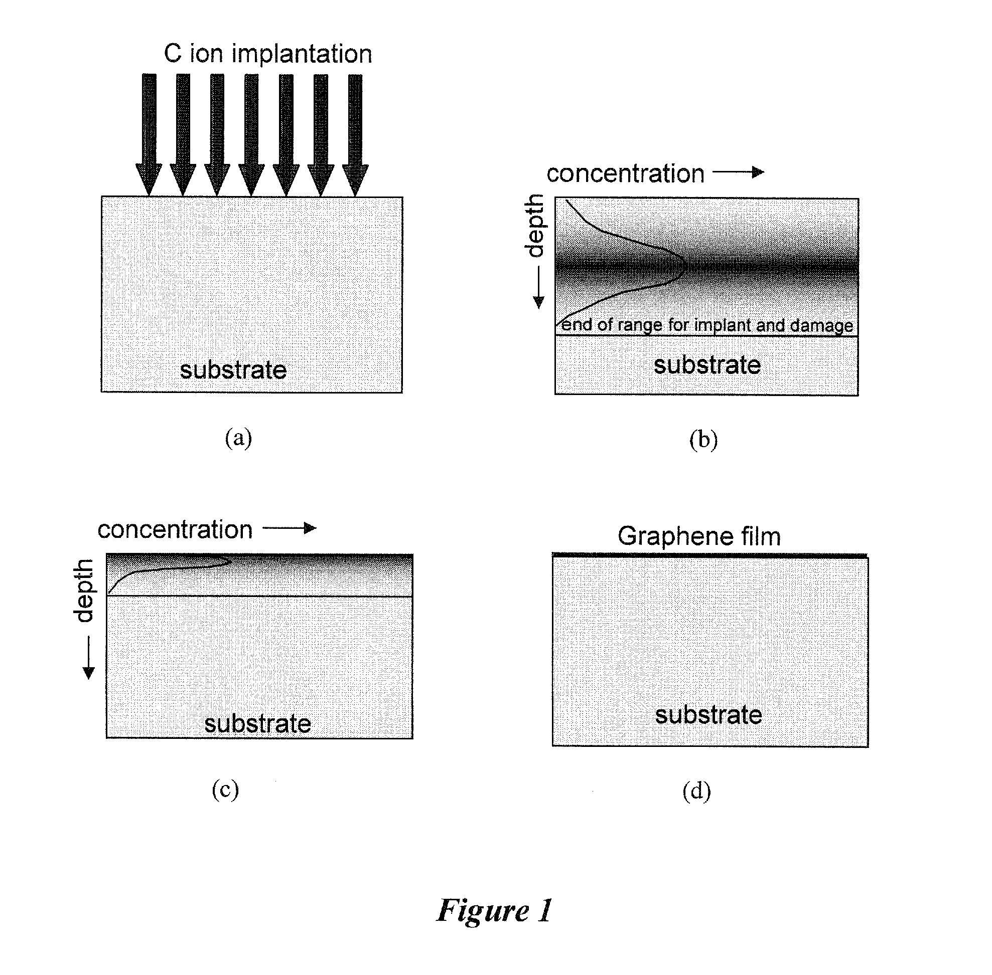
[0010]One embodiments of the invention is directed to methods for fabricating graphene layers of a controlled-thickness over large areas on a substrate. Another embodiment of the invention is directed to methods for fabricated patterned graphene layers of a controlled-thickness. Other embodiments of the invention are directed to devices useful for sensor or other applications that are formed by these methods of forming graphene layers. The devices can be fabricated using conventional semiconductor technologies or ion beam processing methods, see for example Ion Implantation and Beam Processing, J. S. Williams et al., ed., Academic Press 1984, where the graphene layers form single device features or integrated circuits.

[0011]In one embodiment of the invention, solid phase epitaxy (SPE) is employed on a substrate that has ion implanted carbon. By heating a single crystalline carbon implanted silicon or germanium in the volume near the surface to elevated temperatures, for example 500°...


PUM

PropertyMeasurementUnit
Temperatureaaaaaaaaaa
Thicknessaaaaaaaaaa
Volumeaaaaaaaaaa

Abstract

A supported graphene device comprises at least one graphene feature of 1 to about 10 graphene layers having a predetermined shape and pattern, with at least a portion of each graphene feature being supported on a substrate. In some embodiments the device comprises graphene features supported on crystalline semiconductor substrate, such as silicon or germanium. The graphene features on a crystalline semiconductor substrate can be fabricated by forming an amorphous carbon doped semiconductor on the crystalline semiconductor substrate and then epitaxially crystallizing the amorphous semiconductor with carbon migration to the surface to form a graphene feature of one or more graphene layers. The epitaxy can be promoted by heating the device or by irradiation with a laser. Methods for fabricating graphene on a variety of substrates, over large areas with controlled thicknesses employ ion implantation or other doping techniques followed by pulsed laser annealing or other annealing techniques that result in solid phase regrowth are presented.

Description


Claims


Application Information

Patent Timeline
Owner UNIV OF FLORIDA RES FOUNDATION INC
Why Eureka
Try Eureka