Method of manufacturing semiconductor device

a manufacturing method and semiconductor technology, applied in the direction of semiconductor devices, basic electric elements, electrical equipment, etc., can solve the problems of insufficient performance, increased leak current, and difficulty in implementing techniques, so as to reduce parasitic resistance, increase leak current, and promote the effect of silicacidation reaction

Inactive Publication Date: 2009-12-24
LAPIS SEMICON CO LTD
View PDF2 Cites 185 Cited by
  • Summary
  • Abstract
  • Description
  • Claims
  • Application Information

AI Technical Summary

Benefits of technology

[0014]According to the semiconductor device manufacturing method of the present invention, the upper parts of the side surfaces of the gate electrode are exposed by the etch-back process of the sidewalls of the gate electrode, and the metal film is formed on the exposed parts as well. Hence, while the silicidation reaction is limited in the drain/source regions by the control of the thickness of the metal film, in the gate electrode, the silicidation reaction advances from the sides as well, and thus the silicidation reaction can be promoted even with the thickness of the deposited metal film being thin. By this means, the silicide layer formed on the gate electrode can be made sufficiently thicker than the silicide ...

Problems solved by technology

This lateral silicidation advancement causes pn junctions defining drain/source regions to be damaged, resulting in an increase in leak current.
However, simply making the Co film thinner will also render the silicide layer formed on gate electrodes thinner, and thus the reduction in parasitic resistance will be limited, resulting in insufficient performance.
However, either of them requires a large scale change to the existing salicide process, and it is not necessari...

Method used


Image

  • Method of manufacturing semiconductor device
  • Method of manufacturing semiconductor device
  • Method of manufacturing semiconductor device

Examples


first embodiment

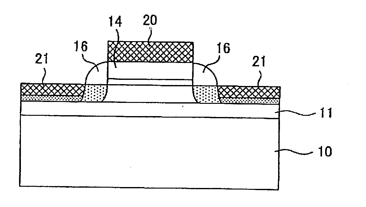
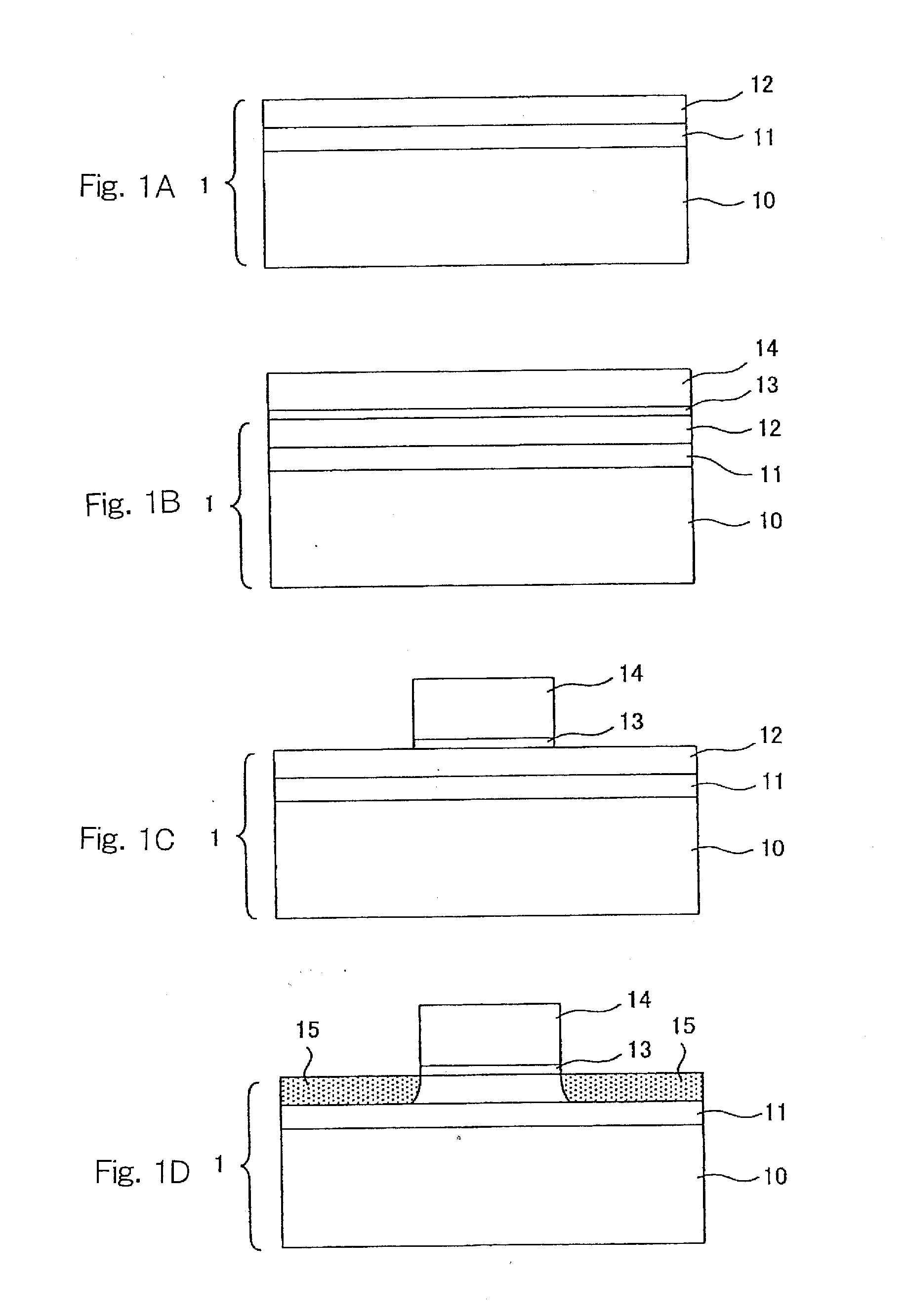
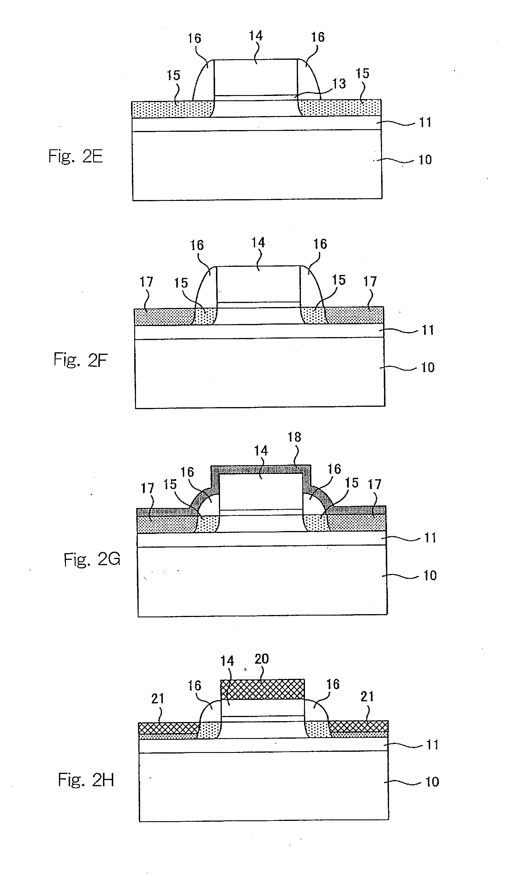
[0017]FIGS. 1A to 1D and FIGS. 2E to 2H are cross-sectional diagrams for the process steps respectively of an SOI-MOSFET manufacture process according to a first embodiment of the present invention.

[0018]First, an SOI substrate 1 constituted by a silicon substrate 10, a BOX layer 11, and a semiconductor layer (SOI layer) 12 laid one over another is prepared. The SOI substrate 1 may be made by any method such as a UNIBOND method (registered trademark), a sticking method, a SIMOX (Silicon Implanted Oxide) method, or the like. In the UNIBOND method, after an oxide film is formed over a surface of a wafer, a high concentration of hydrogen ions are implanted, and another wafer having been stuck to the wafer, the implanted wafer is split (SmartCut) along the hydrogen-ion implanted layer by a thermal process, thereby forming the SOI substrate. In the SIMOX method, a high concentration (e.g., 1E18 cm−2) of oxygen O2 with high energy (e.g., 180 KeV) is ion-implanted into a prime wafer surfac...

second embodiment

[0029]Next, the manufacturing method of MOSFETs using the SOI substrate according to a second embodiment of the present invention will be described with reference to FIGS. 3A to 3C and FIGS. 4D to 4E. The manufacturing method of the present embodiment is the same in the process until the step of forming the poly-silicon film constituting the gate electrodes 14 over the SOI substrate 1 as in the above first embodiment, and description thereof is omitted. Thus, FIGS. 3A to 3C and FIGS. 4D to 4E show the process steps after the poly-silicon film 14 is formed.

[0030]After the SiO2 film 13 constituting a gate oxide film and the poly-silicon film 14 constituting gate electrodes are formed over the SOI substrate 1, a plurality of grooves, e.g., about 0.2 μm wide and about 0.1 μm deep are formed at about 0.2 μm intervals in the gate electrode 14 by photolithography and dry etching. With the plurality of grooves, the surface area of the top of the gate electrode 14 becomes about 1.5 times lar...

third embodiment

[0038]Next, the manufacturing method of MOSFETs using the SOI substrate according to a third embodiment of the present invention will be described with reference to FIGS. 5A to 5C and FIGS. 6D to 6E.

[0039]First, a SiO2 film 13 of about 100 Å thickness constituting a gate oxide film is formed over the semiconductor layer (SOI layer) 12 by the thermal oxidation process. Then, a first poly-silicon film 14a constituting the lower layer of gate electrodes 14 is formed over the SiO2 film 13 by the LP-CVD method or the like. The first poly-silicon film ˜14a is formed by a method usually performed when forming gate electrodes, for example, a reduced-pressure CVD method under process conditions of a reaction temperature of 620° C. and a pressure of 0.2 Torr using silane gas (SiH4). Subsequently, a second poly-silicon film 14b having multiple bumps and hollows on its surface, i.e., having a rough surface is formed over the first poly-silicon film 14a. The second poly-silicon film 14b is const...


PUM


Abstract

A semiconductor device manufacturing method which sequentially forms a gate oxide film and gate electrode material over a semiconductor layer of an SOI substrate and patterns the material into gate electrodes. The method further comprises the steps of forming sidewalls made of an insulator to cover side surfaces of the gate electrode; ion-implanting into the semiconductor layer on both sides of the gate electrode to form drain/source regions; partially etching the sidewalls to expose upper parts of the side surfaces of the gate electrode; depositing a metal film to cover the tops of the drain/source regions and of the gate electrode and the exposed upper parts of the side surfaces of the gate electrode; and performing heat treatment on the SOI substrate to form silicide layers respectively in the surfaces of the gate electrode and of the drain/source regions.

Description

BACKGROUND OF THE INVENTION[0001]1. Technical Field[0002]The present invention relates to a semiconductor device and particularly to a semiconductor device manufacturing method including a process of forming a silicide layer on gate electrodes and drain / source regions of semiconductor devices using an SOI (Silicon on Insulator) substrate.[0003]2. Description of the Related Art[0004]There is an increasing demand for LSIs with low power consumption and high performance for product applications related to personal mobile communications. However, usual CMOS devices using a silicon substrate are increasing in power consumption due to becoming more highly integrated and higher in speed with circuit elements becoming finer in size, and hence it is desired that new low power devices with a new device structure be developed. In this situation, SOI devices using an SOI (Silicon On Insulator) substrate having an insulating film between a silicon substrate and a device area are expected to serv...

Claims


Application Information

Patent Timeline
IPC IPC(8): H01L21/336
CPCH01L21/28052H01L29/42384H01L29/458H01L29/6653H01L29/4975H01L29/665H01L29/4908
Inventor OKIHARA, MASAO
Owner LAPIS SEMICON CO LTD
Why Eureka
Try Eureka