Control of dopant diffusion from buried layers in bipolar integrated circuits

a bipolar integrated circuit and dopant diffusion technology, applied in the field of semiconductor integrated circuits, can solve the problems of significant dopant concentration gradient, reduced effective collector resistance, and relatively resistive light-doped subcollectors, and achieve the effect of reducing the diffusion of dopan

Inactive Publication Date: 2005-11-10
BABCOCK JEFFREY A +5
View PDF2 Cites 173 Cited by
  • Summary
  • Abstract
  • Description
  • Claims
  • Application Information

AI Technical Summary

Benefits of technology

[0014] It is therefore an object of the present invention to provide an integrated circuit and method of fabricatio

Problems solved by technology

These lightly-doped subcollectors are relatively resistive, however.
Therefore, many modern bipolar structures reduce the effective collector resistance by providing a heavily-doped buried collector layer underlying the subcollector.
This construction results in a significant dopant concentration gradient at the interface between the buried collector regions and the much more lightly-doped overlying subcollector.
A particularly troublesome high temperature process is the epitaxial formation of the subcollector itself, which exposes the wafer to high temperatures for a relatively long period of time.
This updiffusion of dopant from the buried collector can cause significant limitations in the performance and precision of modern bipolar circuits.
Efforts to reduce this updiffusion are known to have detrimental device effects.
Increasing the thickness of epitaxial layer 8 to compensate for the updiffusion effect not only exacerbates the diffusion itself (by increasing the time or temperature of the process), but also is incompatible with the fabrication of high performance and high-speed devices.
Not only does the undesired diffusion from each buried layer reduce the performance of individual transistors 10m 10n, but the difference in diffusion rate also causes mismatch between the complementary transistors in a given circuit.
This mismatch renders the delicate balance of the tradeoff between NPN and PNP performance, and the necessary optimization techniques, even more difficult.
Besides compromising the ultimate performance of the circuit, this device type asymmetry also can reduce the power

Method used


Image

  • Control of dopant diffusion from buried layers in bipolar integrated circuits
  • Control of dopant diffusion from buried layers in bipolar integrated circuits
  • Control of dopant diffusion from buried layers in bipolar integrated circuits

Examples


Embodiment Construction

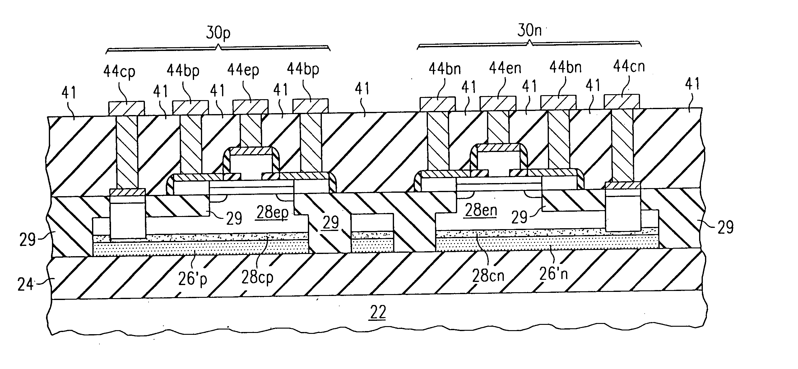
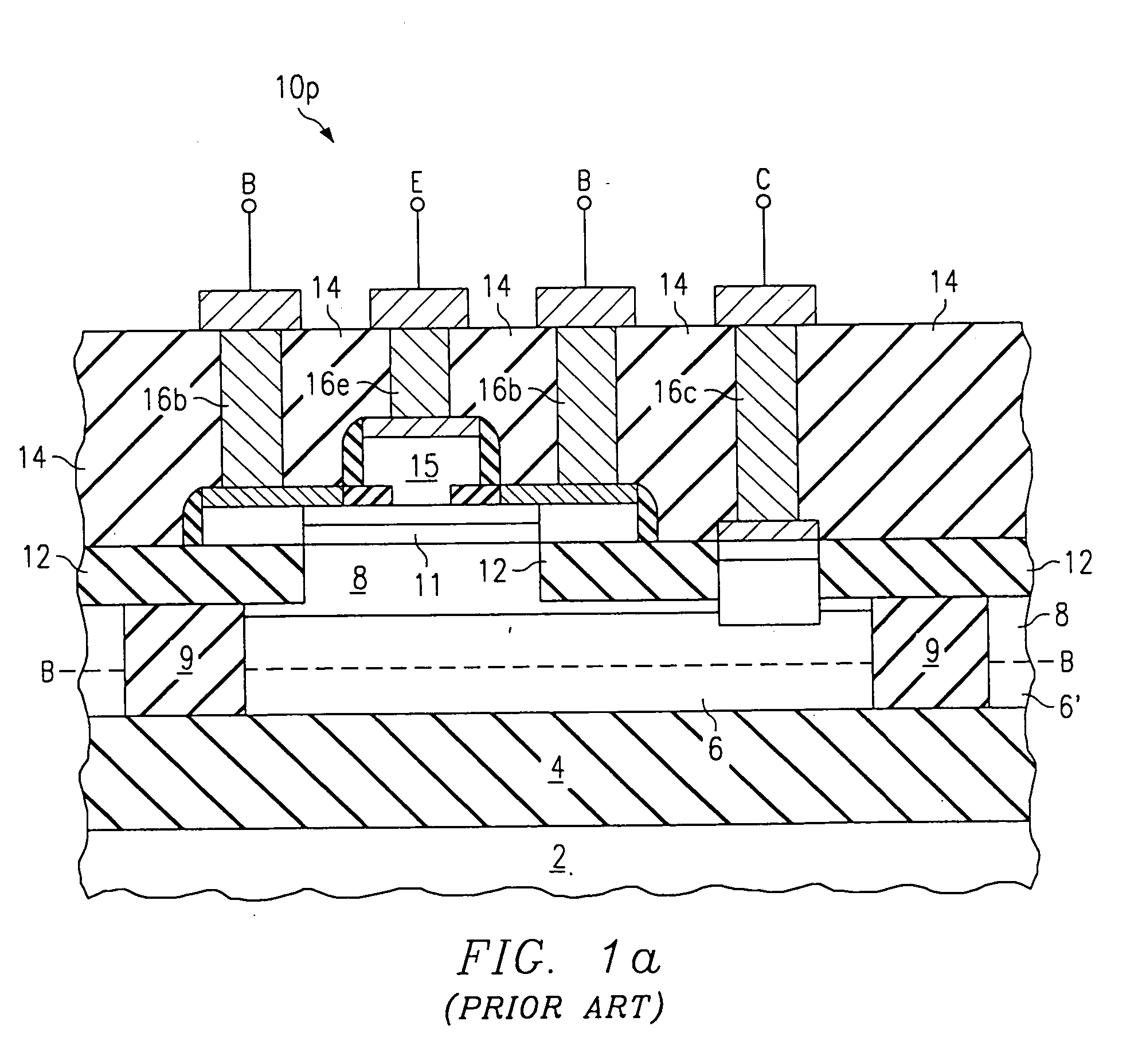
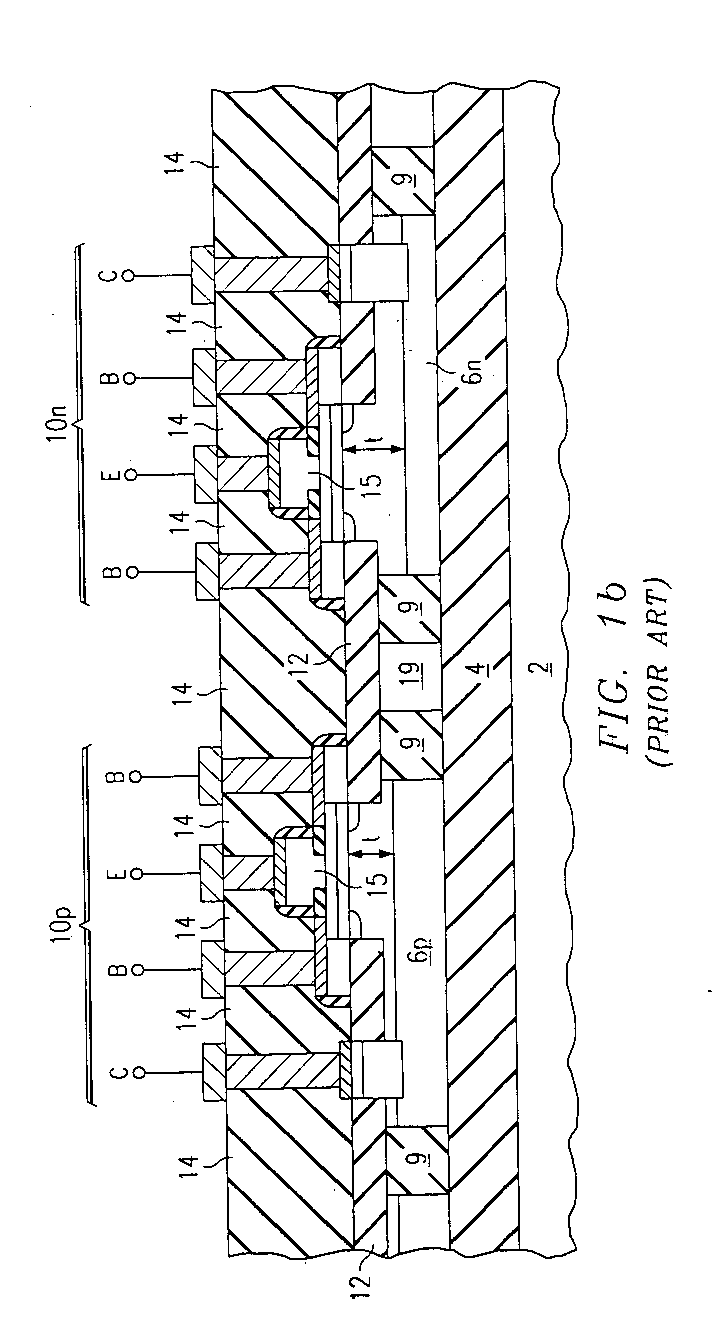
[0028] The present invention will now be described in connection with its preferred embodiments. These exemplary embodiments are directed to the fabrication of bipolar junction transistors in a silicon-on-insulator (SOI) structure. It will be appreciated by those skilled in the art having reference to this specification that the present invention may be used to form either p-n-p or n-p-n transistors, or both as may be used in a complementary bipolar or BiCMOS technology, as well as used in other alternative structures and methods of fabricating such structures. In addition, while this invention is particularly beneficial as applied to SOI structures, it is also contemplated that this invention may be utilized in bulk integrated circuit devices as well, where no buried insulator layer is present. Furthermore, while these embodiments are silicon or SiGe NPN and PNP bipolar transistors, it is contemplated that the present invention will be equally applicable to emerging bipolar technol...


PUM


Abstract

An integrated circuit and method of fabricating the integrated circuit is disclosed. The integrated circuit includes vertical bipolar transistors (30, 50, 60), each having a buried collector region (26′). A carbon-bearing diffusion barrier (28c) is disposed over the buried collector region (26′), to inhibit the diffusion of dopant from the buried collector region (26′) into the overlying epitaxial layer (28). The diffusion barrier (28c) may be formed by incorporating a carbon source into the epitaxial formation of the overlying layer (28), or by ion implantation. In the case of ion implantation of carbon or SiGeC, masks (52, 62) may be used to define the locations of the buried collector regions (26′) that are to receive the carbon; for example, portions underlying eventual collector contacts (33, 44c) may be masked from the carbon implant so that dopant from the buried collector region (26′) can diffuse upward to meet the contact (33). MOS transistors (70, 80) including the diffusion barrier (28) are also disclosed.

Description

CROSS-REFERENCE TO RELATED APPLICATIONS [0001] Not applicable. STATEMENT REGARDING FEDERALLY SPONSORED RESEARCH OR DEVELOPMENT [0002] Not applicable. BACKGROUND OF THE INVENTION [0003] This invention is in the field of semiconductor integrated circuits, and is more specifically directed to the formation of buried doped layers in bipolar transistors in such circuits. [0004] Modern bipolar integrated circuits now typically use vertical bipolar transistors as their active elements. These transistors are vertical in the sense that the active base and emitter regions overlie the collector region, with collector-emitter current traveling through the base in substantially a vertical orientation relative to the plane of the surface of the integrated circuit at which the transistor resides. To provide a robust breakdown voltage, the portion of the collector region adjacent the base is relatively lightly doped. This region is often referred to as the “subcollector”. These lightly-doped subcol...

Claims


Application Information

Patent Timeline
IPC IPC(8): H01L21/331H01L21/8222H01L21/8228H01L29/73H01L29/737
CPCH01L21/82285H01L29/66242H01L29/7378H01L29/7317H01L29/66265
Inventor BABCOCK, JEFFREY A.PINTO, ANGELOSCHIEKOFER, MANFREDBALSTER, SCOTT G.HOWARD, GREGORY E.HAUSLER, ALFRED
Owner BABCOCK JEFFREY A
Why Eureka
Try Eureka